عضویت
عضویت  ورود اعضا
 راهنمای خرید


ADP2165/ADP2166: 5.5 V, 5A/6A, High Efficiency, Step-Down DC-to-DC Regulators with Output Tracking Data Sheet0 pages
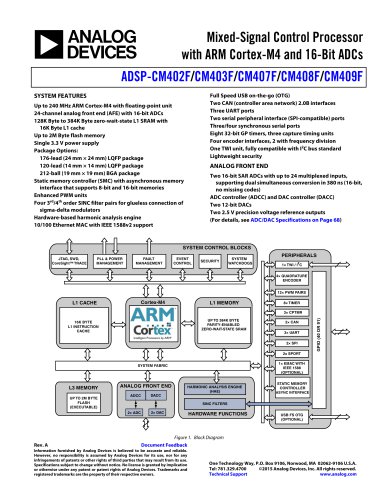
TYPICAL APPLICATION CIRCUIT
Continuous output current
ADP2165: 5 A
ADP2166: 6 A
Integrated MOSFET
High-side on resistance: 19 mΩ
Low-side on resistance: 15 mΩ
Reference voltage: 0.6 V ± 1% over temperature range
Input voltage range: 2.7 V to 5.5 V
Current mode architecture
Switching frequency
Fixed frequency: 620 kHz or 1.2 MHz
Adjustable frequency: 250 kHz to 1.4 MHz
Synchronizes to external clock: 250 kHz to 1.4 MHz
Selectable synchronize phase shift: in phase or out of phase
External compensation
Programmable soft start
Startup into a precharged output
Voltage tracking input
Power-good output and precision enable input
Accurate current limit
Available in 24-lead, 4 mm × 4 mm LFCSP_WQ package
Supported by ADIsimPower™ design tool
APPLICATIONS
Point of load regulation
Communications and networking
High end consumer
Industrial, instrumentation, and healthcare
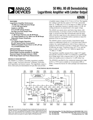
BST
CBST
AVIN
CIN
VOUT
PGOOD
RTOP
SYNC
RRT
COUT
FB
RT
CVREG
L1
SW
EN
COMP
TRK
SS
VREG
GND
PGND
CCP
CSS
RC
RBOT
CC
Figure 1.
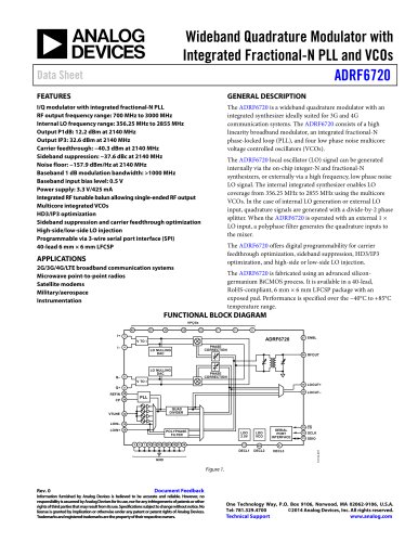
The ADP2165/ADP2166 are designed to be extremely flexible
with the addition of a minimal amount of external components
to program soft start and control loop compensation.
The ADP2165/ADP2166 are supplied from an input voltage of
2.7 V to 5.5 V. Output voltage options include 3.3 V, 2.5 V, 1.8 V,
1.5 V, 1.2 V, or 1.0 V fixed outputs and adjustable options capable
of supporting an output voltage range from 0.6 V to 90% of the
input voltage. Protection features include undervoltage lockout
(UVLO), overvoltage protection (OVP), overcurrent protection
(OCP), and thermal shutdown (TSD) for robust performance.
The ADP2165/ADP2166 operate over the −40°C to +125°C
junction temperature range and are available in a 24-lead
LFCSP_WQ package.
GENERAL DESCRIPTION
100
Key features include precision enable, power-good monitor,
and output voltage tracking to facilitate robust sequencing.
The switching frequency can be programmed from 250 kHz
to 1.4 MHz, or it can be fixed at 620 kHz or 1.2 MHz. The
synchronization function allows the switching frequency to
synchronize to an external clock, minimizing the
electromagnetic interference (EMI) of the system.
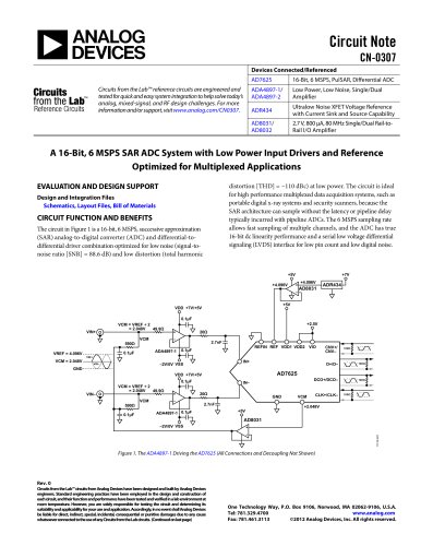
VPVIN = 3.3V
95
90
VPVIN = 5V
85
EFFICIENCY (%)
The ADP2165/ADP2166 are high efficiency, current mode
control, step-down dc-to-dc regulators with an integrated 19 mΩ
high-side FET and a 15 mΩ synchronous rectified FET. The
ADP2165/ADP2166 combine a small size, 4 mm × 4 mm LFCSP
package with an accurate current limit, resulting in a smaller
inductor size and a high power density, point of load solution.
Rev. 0
ADP2165/
ADP2166
PVIN
VPVIN
10956-001
FEATURES
80
75
70
65
60
55
VOUT = 1.8V
fSW = 600kHz
50
0
1
2
3
4
OUTPUT CURRENT (A)
5
6
10956-002
Data Sheet
5.5 V, 5 A/6 A, High Efficiency, Step-Down
DC-to-DC Regulators with Output Tracking
ADP2165/ADP2166
Figure 2. Efficiency vs. Output Current
Document Feedback
Information furnished by Analog Devices is believed to be accurate and reliable. However, no
responsibility is assumed by Analog Devices for its use, nor for any infringements of patents or other
rights of third parties that may result from its use. Specifications subject to change without notice. No
license is granted by implication or otherwise under any patent or patent rights of Analog Devices.
Trademarks and registered trademarks are the property of their respective owners.
One Technology Way, P.O. Box 9106, Norwood, MA 02062-9106, U.S.A.
Tel: 781.329.4700
©2014 Analog Devices, Inc. All rights reserved.
Technical Support
www.analog.com