عضویت
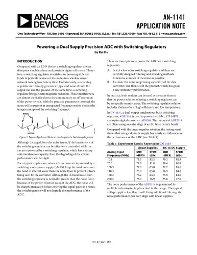
عضویت  ورود اعضا
 راهنمای خرید


ADP2311:Dual 1 A, 18 V, Synchronous Step-Down Regulator with Fail-Safe Voltage Monitoring0 pages
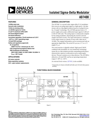
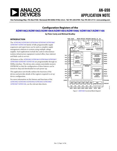
Dual 1 A, 18 V, Synchronous Step-Down
Regulator with Fail-Safe Voltage Monitoring
ADP2311
Data Sheet
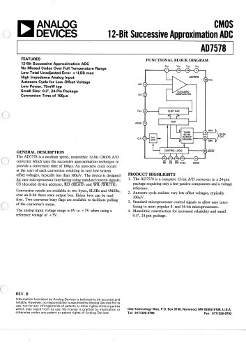
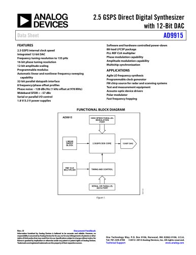
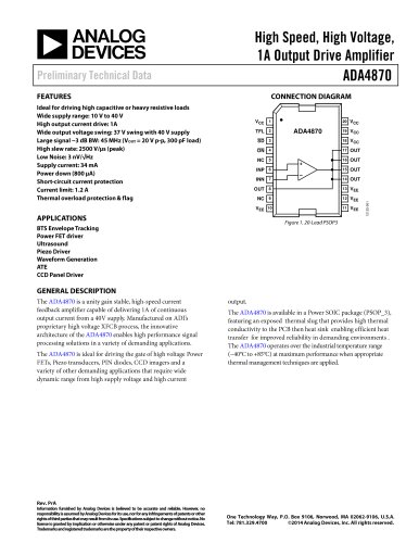
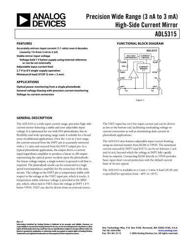
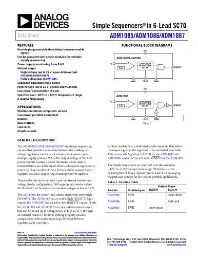
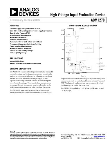
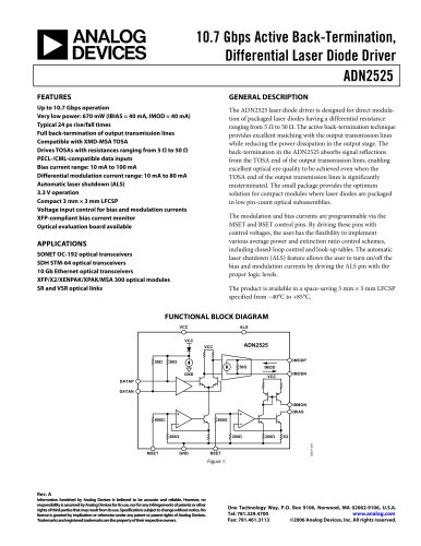
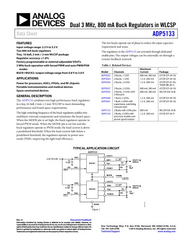
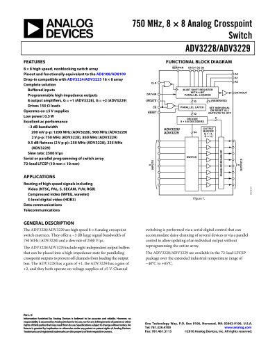
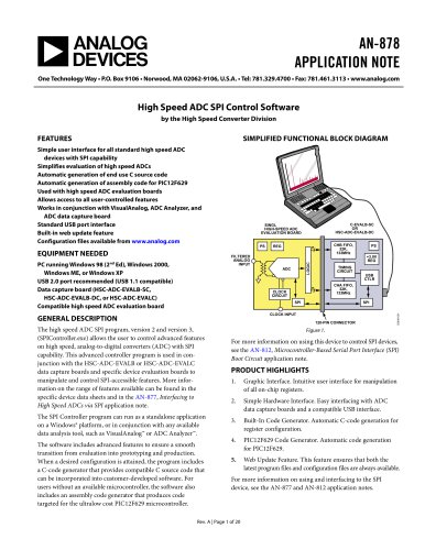
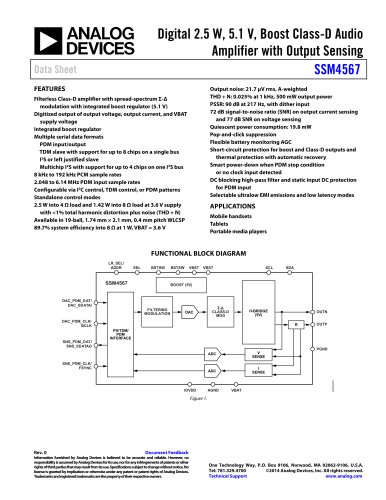
TYPICAL APPLICATION CIRCUIT
Input voltage: 4.5 V to 18 V
±1.0% output accuracy
Integrated MOSFET: 110 mΩ/60 mΩ typical
Continuous output current: 1 A/1 A
Power fail comparator generates warning
Power-on reset with programmable delay timer
Adjustable voltage monitor for power-down (Channel 2)
Watchdog refresh input
Dual phase with 180° out-of-phase operation
Fixed switching frequency: 300 kHz
Internal compensation and soft start
Stable with low ESR output ceramic capacitors
Precision enable input
Power feedback during power-off
UVLO, OCP, OVP, and thermal shutdown protection
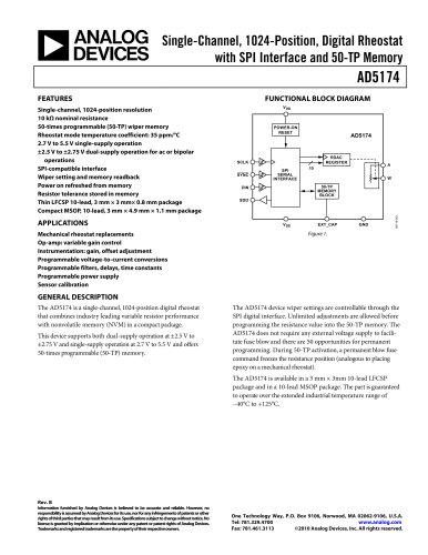
PFO POR WDI
EN
PVIN1
VIN
RSTO
RVM2_TOP
PFI
CIN2
VM2
RPFI_BOT
RVM2_BOT
BST1
C1BST
VOUT1
VIN
PVIN2
RPFI_TOP
CIN1
ADP2311
BST2
SW2
PGND2
SW1
PGND1
RTOP1
COUT1
C2BST
L2
L1
FB1
RBOT1
RTOP2
VOUT2
COUT2
FB2
GND VREG
TIMER
CVREG
RBOT2
11036-001
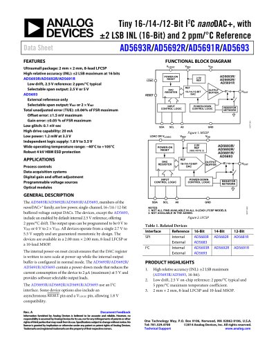
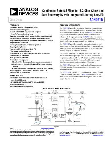
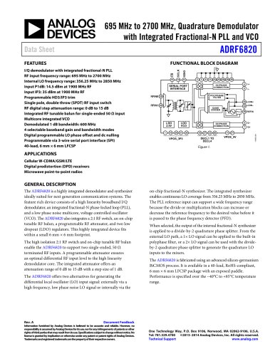
FEATURES
CTIMER
Figure 1.
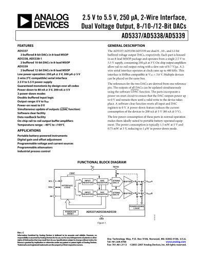
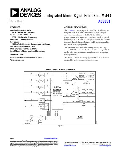
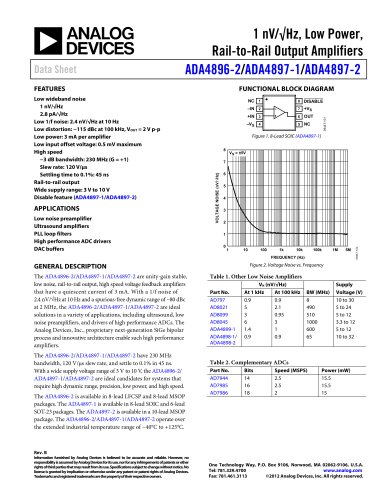
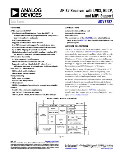
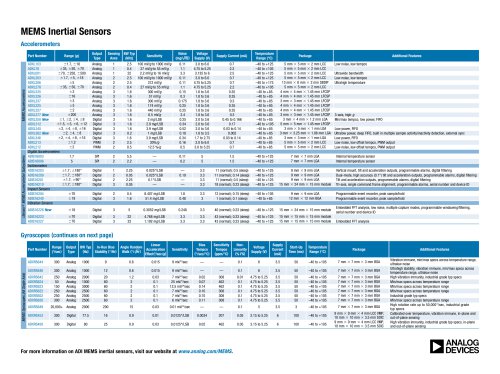
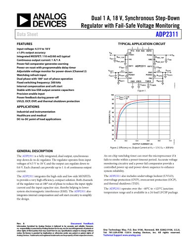
100
VOUT = 3.3V
VOUT = 5V
95
90
APPLICATIONS
EFFICIENCY (%)
85
Industrial and instrumentation
Healthcare and medical
DC-to-DC point of load applications
80
75
70
65
60
50
0
0.2
0.4
0.6
0.8
1.0
OUTPUT CURRENT (A)
11036-002
55
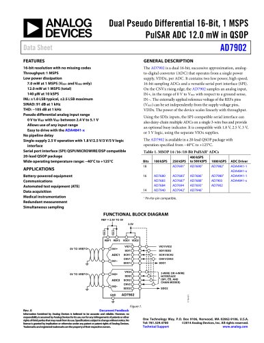
Figure 2. Efficiency vs. Output Current at VIN = 12 V, fSW = 300 kHz
GENERAL DESCRIPTION
The ADP2311 is a fully integrated, dual output, synchronous
step-down dc-to-dc regulator. The regulator operates from input
voltages of 4.5 V to 18 V, and the output can regulate down to
0.6 V. Each channel can provide up to 1 A of continuous output
current.
An on-chip watchdog timer can reset the microprocessor if it
fails to strobe within a preset timeout period. Accurate voltage
monitoring circuitry and a power fail comparator provide a
controlled power-up and power-down sequence to enhance
system reliability.
The ADP2311 integrates the high-side and low-side MOSFETs
to provide a very high efficiency, compact solution. Both channels
of the regulator run at 180° out of phase to reduce the input ripple
current and the input capacitor size, thereby helping to lower
system electromagnetic interference (EMI). The ADP2311 also
integrates internal compensation and soft start circuitry to simplify
the design.
The ADP2311 also includes undervoltage lockout (UVLO),
overvoltage protection (OVP), overcurrent protection (OCP),
and thermal shutdown (TSD).
Rev. A
The ADP2311 operates over the −40°C to +125°C junction
temperature range and is available in a 24-lead LFCSP package.
Document Feedback
Information furnished by Analog Devices is believed to be accurate and reliable. However,
no responsibility is assumed by Analog Devices for its use, nor for any infringements of patents or
other rights of third parties that may result from its use. Specifications subject to change without
notice. No license is granted by implication or otherwise under any patent or patent rights of
Analog Devices. Trademarks and registered trademarks are the property of their respective owners.
One Technology Way, P.O. Box 9106, Norwood, MA 02062-9106, U.S.A.
Tel: 781.329.4700 ©2014 Analog Devices, Inc. All rights reserved.
Technical Support www.analog.com