عضویت
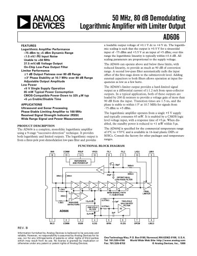
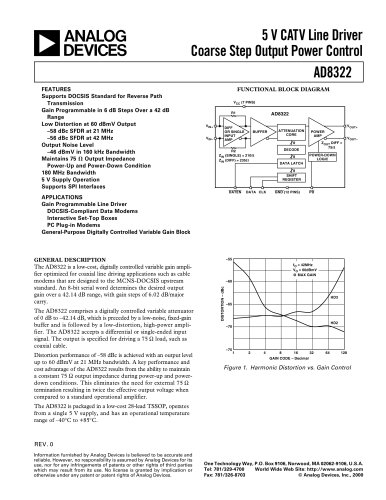
عضویت  ورود اعضا
 راهنمای خرید


ADP5133: Dual 3 MHz, 800 mA Buck Regulators in WLCSP0 pages
Dual 3 MHz, 800 mA Buck Regulators in WLCSP
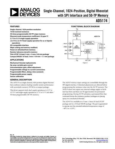
ADP5133
Data Sheet
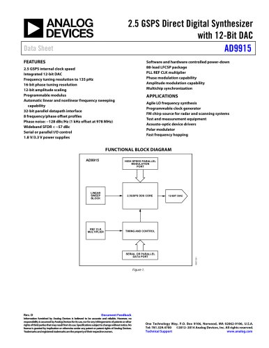
FEATURES
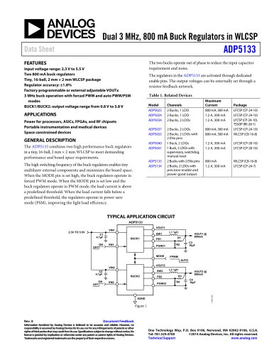
The two bucks operate out of phase to reduce the input capacitor
requirement and noise.
Input voltage range: 2.3 V to 5.5 V
Two 800 mA buck regulators
Tiny, 16-ball, 2 mm × 2 mm WLCSP package
Regulator accuracy: ±1.8%
Factory programmable or external adjustable VOUTx
3 MHz buck operation with forced PWM and auto PWM/PSM
modes
BUCK1/BUCK2: output voltage range from 0.8 V to 3.8 V
The regulators in the ADP5133 are activated through dedicated
enable pins. The output voltages can be externally set through a
resistor feedback network.
Table 1. Related Devices
Maximum
Current
800 mA, 300 mA
1.2 A, 300 mA
1.2 A, 300 mA
Model
ADP5023
ADP5024
ADP5034
ADP5037
ADP5033
APPLICATIONS
Power for processors, ASICs, FPGAs, and RF chipsets
Portable instrumentation and medical devices
Space constrained devices
GENERAL DESCRIPTION
Channels
2 Bucks, 1 LDO
2 Bucks, 1 LDO
2 Bucks, 2 LDOs
2 Bucks, 2 LDOs
2 Bucks, 2 LDOs with
2 ENx pins
1 Buck, 2 LDOs
1 Buck, 2 LDOs with
supervisory, watchdog,
manual reset
2 Bucks with 2 ENx pins
2 Bucks, 2 LDOs with
precision enable and
power-good output
ADP5040
ADP5041
The ADP5133 combines two high performance buck regulators
in a tiny, 16-ball, 2 mm × 2 mm WLCSP to meet demanding
performance and board space requirements.
ADP5133
ADP5134
The high switching frequency of the buck regulators enables tiny
multilayer external components and minimizes the board space.
When the MODE pin is set high, the buck regulators operate in
forced PWM mode. When the MODE pin is set low and the
buck regulators operate in PWM mode, the load current is above
a predefined threshold. When the load current falls below a
predefined threshold, the regulators operate in power save
mode (PSM), improving the light load efficiency.
800 mA, 300 mA
800 mA, 300 mA
Package
LFCSP (CP-24-10)
LFCSP (CP-24-10)
LFCSP (CP-24-10),
TSSOP (RE-28-1)
LFCSP (CP-24-10)
WLCSP (CB-16-8)
1.2 A, 300 mA
1.2 A, 300 mA
LFCSP (CP-20-10)
LFCSP (CP-20-10)
800 mA
1.2 A, 300 mA
WLCSP (CB-16-8)
LFCSP (CP-24-7)
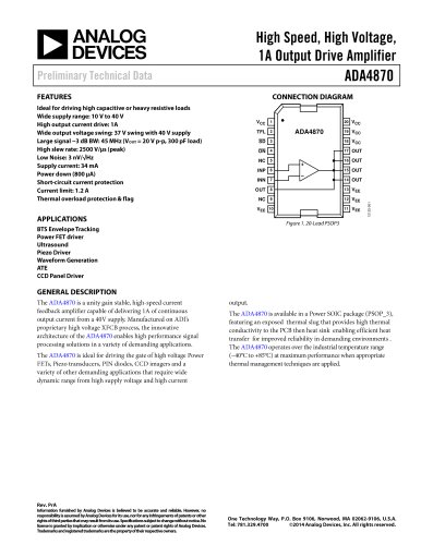
TYPICAL APPLICATION CIRCUIT
ADP5133
VOUT1
2.3V TO 5.5V
VIN1
SW1
C1
4.7µF
ON
BUCK1
EN1
FB1
PGND1
OFF
MODE
L1 1µH
R1
VOUT1 @
800mA
C3
10µF
R2
FPWM
AUTO
VOUT2
VIN2
SW2
ON
OFF
BUCK2
EN2
FB2
PGND2
AGND
L2 1µH
R3
R4
VOUT2 @
800mA
C4
10µF
11991-001
C2
4.7µF
Figure 1.
Rev. 0
Document Feedback
Information furnished by Analog Devices is believed to be accurate and reliable. However, no
responsibility is assumed by Analog Devices for its use, nor for any infringements of patents or other
rights of third parties that may result from its use. Specifications subject to change without notice. No
license is granted by implication or otherwise under any patent or patent rights of Analog Devices.
Trademarks and registered trademarks are the property of their respective owners.
One Technology Way, P.O. Box 9106, Norwood, MA 02062-9106, U.S.A.
Tel: 781.329.4700
©2014 Analog Devices, Inc. All rights reserved.
Technical Support
www.analog.com