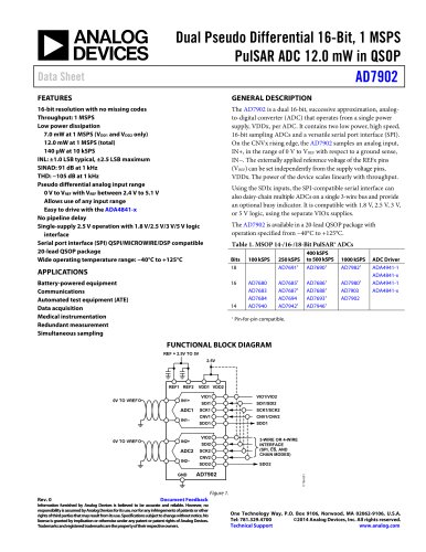
عضویت
عضویت  ورود اعضا
 راهنمای خرید


AD5693R/AD5692R/AD5691R/AD5693: Tiny 16-/14-/12-Bit I2C nanoDAC+, with ±2 LSB INL (16-Bit) and 2 ppm/°C Reference0 pages
Tiny 16-/14-/12-Bit I2C nanoDAC+, with
±2 LSB INL (16-Bit) and 2 ppm/°C Reference
AD5693R/AD5692R/AD5691R/AD5693
Data Sheet
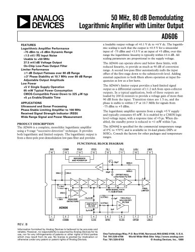
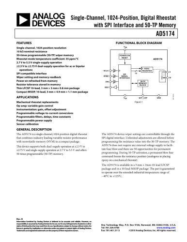
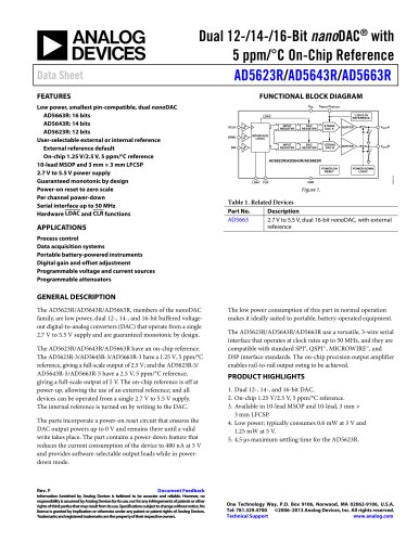
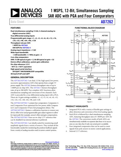
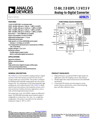
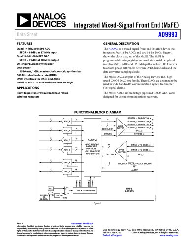
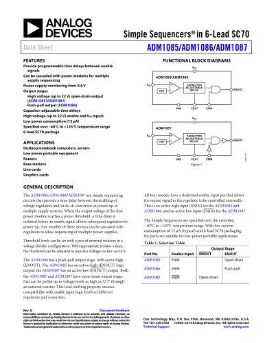
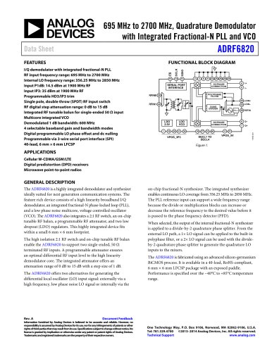
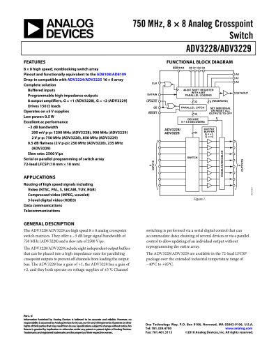
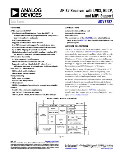
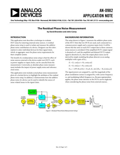
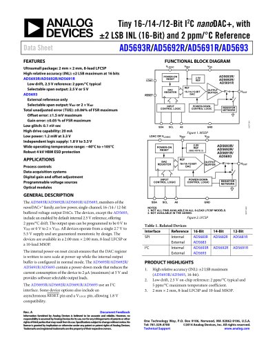
FUNCTIONAL BLOCK DIAGRAM
Ultrasmall package: 2 mm × 2 mm, 8-lead LFCSP
High relative accuracy (INL): ±2 LSB maximum at 16 bits
AD5693R/AD5692R/AD5691R
Low drift, 2.5 V reference: 2 ppm/°C typical
Selectable span output: 2.5 V or 5 V
AD5693
External reference only
Selectable span output: VREF or 2 × VREF
Total unadjusted error (TUE): ±0.06% of FSR maximum
Offset error: ±1.5 mV maximum
Gain error: ±0.05 % of FSR maximum
Low glitch: 0.1 nV-sec
High drive capability: 20 mA
Low power: 1.2 mW at 3.3 V
Independent logic supply: 1.8 V to 5.5 V
Wide operating temperature range: −40°C to +105°C
Robust 4 kV HBM ESD protection
VREF
VLOGIC
VDD
POWER-ON
RESET
LDAC
REF
DAC
REGISTER
16-/14-/12-BIT
DAC
RESET
INPUT
CONTROL LOGIC
SDA
SCL
AD5693R/
AD5692R/
AD5691R
2.5V
REF
OUTPUT
BUFFER
POWER-DOWN
CONTROL LOGIC
VOUT
RESISTOR
NETWORK
12077-001
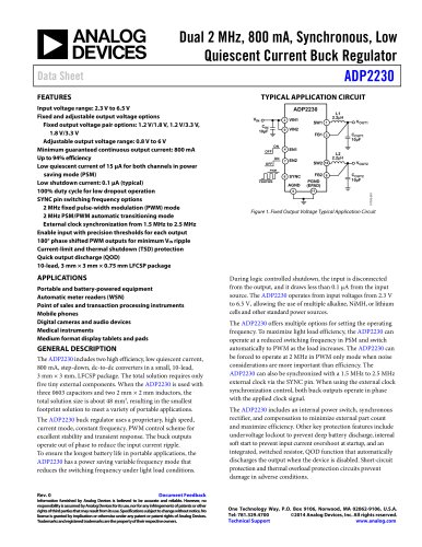
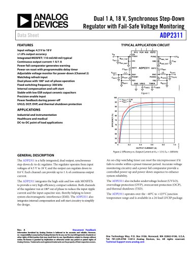
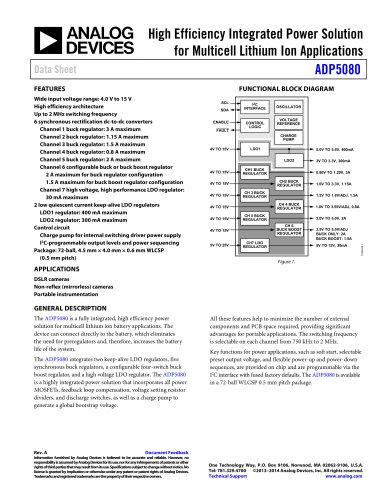
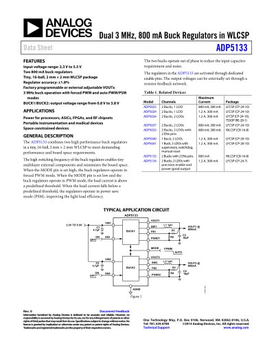
FEATURES
GND
A0
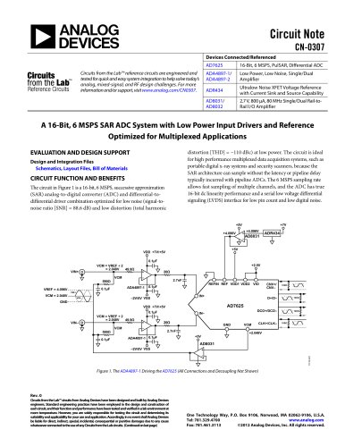
Figure 1. MSOP
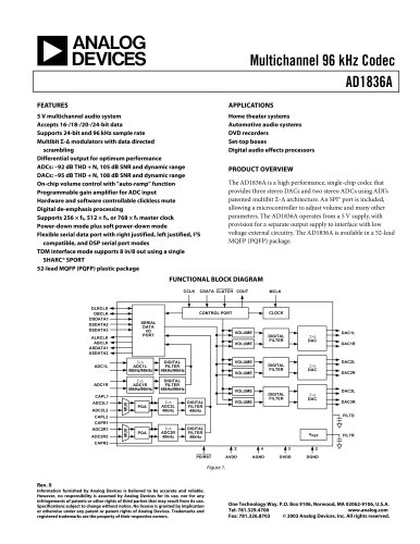
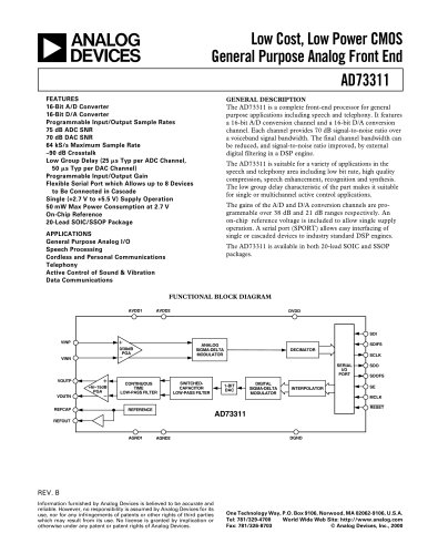
VREF
LDAC OR VLOGIC
VDD
2.5V
REF
POWER-ON
RESET
APPLICATIONS
REF
DAC
REGISTER
Process controls
Data acquisition systems
Digital gain and offset adjustment
Programmable voltage sources
Optical modules
AD5693R/
AD5692R/
AD5691R/
AD5693
(SEE NOTE 2)
16-/14-/12-BIT
DAC
INPUT
CONTROL LOGIC
OUTPUT
BUFFER
POWER-DOWN
CONTROL LOGIC
VOUT
RESISTOR
NETWORK
GENERAL DESCRIPTION
The internal power-on reset circuit ensures that the DAC register
is written to zero scale at power-up while the internal output
buffer is configured in normal mode. The AD5693R/AD5692R/
AD5691R/AD5693 contain a power-down mode that reduces the
current consumption of the device to 2 µA (maximum) at 5 V and
provides software selectable output loads.
The AD5693R/AD5692R/AD5691R/AD5693 use an I2C
interface. Some device options also include an
asynchronous RESET pin and a VLOGIC pin, allowing 1.8 V
compatibility.
Rev. A
SDA
SCL
GND
A0
12077-002
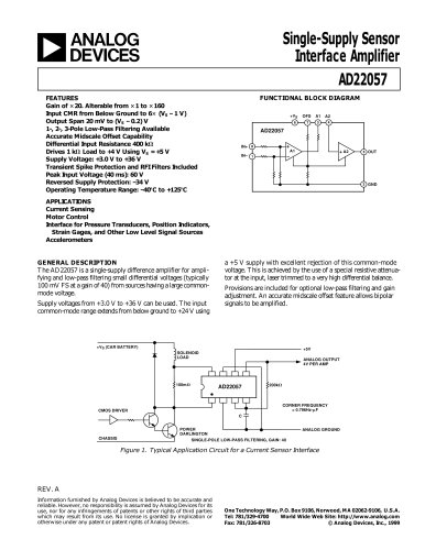
The AD5693R/AD5692R/AD5691R/AD5693, members of the
nanoDAC+® family, are low power, single-channel, 16-/14-/ 12-bit
buffered voltage output DACs. The devices, except the AD5693,
include an enabled by default internal 2.5 V reference, offering
2 ppm/°C drift. The output span can be programmed to be 0 V to
VREF or 0 V to 2 × VREF. All devices operate from a single 2.7 V to
5.5 V supply and are guaranteed monotonic by design. The
devices are available in a 2.00 mm × 2.00 mm, 8-lead LFCSP or
a 10-lead MSOP.
NOTES
1. NOT ALL PINS AVAILABLE IN ALL 8-LEAD LFCSP MODELS.
2. NOT AVAILABLE IN THE AD5693.
Figure 2. LFCSP
Table 1. Related Devices
Interface
SPI
I2 C
Reference
Internal
External
Internal
External
16-Bit
AD5683R
AD5683
AD5693R
AD5693
14-Bit
AD5682R
12-Bit
AD5681R
AD5692R
AD5691R
PRODUCT HIGHLIGHTS
1.
2.
3.
High relative accuracy (INL): ±2 LSB maximum
(AD5693R/AD5693, 16-bit).
Low drift, 2.5 V on-chip reference: 2 ppm/°C typical and
5 ppm/°C maximum temperature coefficient.
2 mm × 2 mm, 8-lead LFCSP and 10-lead MSOP.
Document Feedback
Information furnished by Analog Devices is believed to be accurate and reliable. However, no
responsibility is assumed by Analog Devices for its use, nor for any infringements of patents or other
rights of third parties that may result from its use. Specifications subject to change without notice. No
license is granted by implication or otherwise under any patent or patent rights of Analog Devices.
Trademarks and registered trademarks are the property of their respective owners.
One Technology Way, P.O. Box 9106, Norwood, MA 02062-9106, U.S.A.
Tel: 781.329.4700
©2014 Analog Devices, Inc. All rights reserved.
Technical Support
www.analog.com