عضویت
عضویت  ورود اعضا
 راهنمای خرید


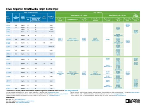
AD7902: Dual Pseudo Differential 16-Bit, 1 MSPS PulSAR ADC 12.0 mW0 pages
Dual Pseudo Differential 16-Bit, 1 MSPS
PulSAR ADC 12.0 mW in QSOP
AD7902
Data Sheet
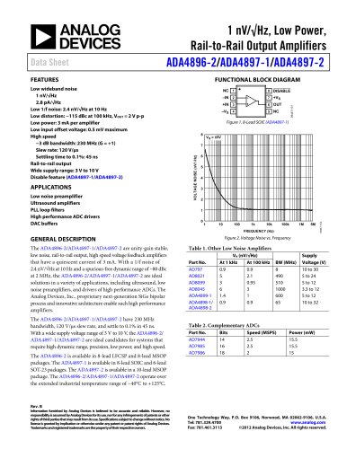
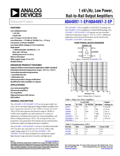
FEATURES
GENERAL DESCRIPTION
16-bit resolution with no missing codes
Throughput: 1 MSPS
Low power dissipation
7.0 mW at 1 MSPS (VDD1 and VDD2 only)
12.0 mW at 1 MSPS (total)
140 μW at 10 kSPS
INL: ±1.0 LSB typical, ±2.5 LSB maximum
SINAD: 91 dB at 1 kHz
THD: −105 dB at 1 kHz
Pseudo differential analog input range
0 V to VREF with VREF between 2.4 V to 5.1 V
Allows use of any input range
Easy to drive with the ADA4841-x
No pipeline delay
Single-supply 2.5 V operation with 1.8 V/2.5 V/3 V/5 V logic
interface
Serial port interface (SPI) QSPI/MICROWIRE/DSP compatible
20-lead QSOP package
Wide operating temperature range: −40°C to +125°C
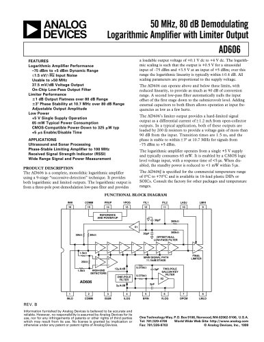
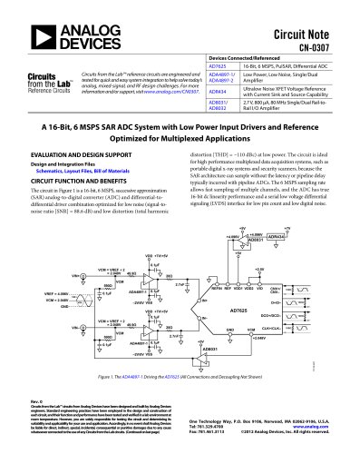
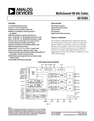
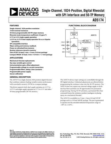
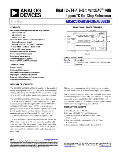
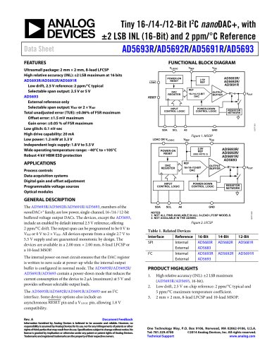
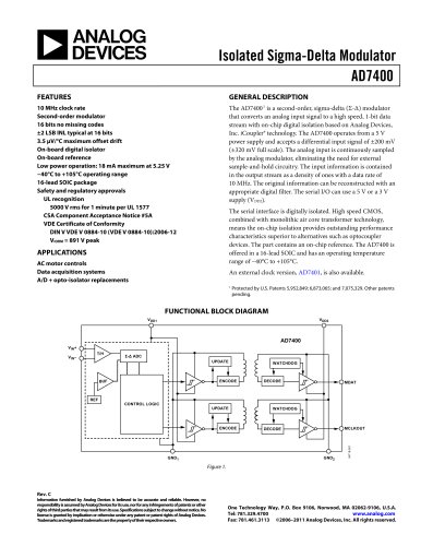
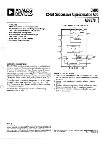
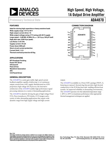
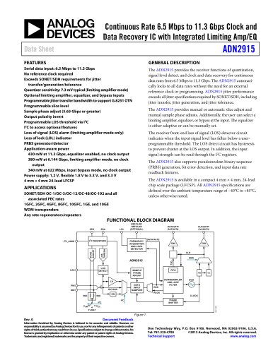
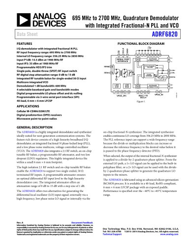
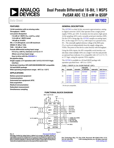
The AD7902 is a dual 16-bit, successive approximation, analogto-digital converter (ADC) that operates from a single power
supply, VDDx, per ADC. It contains two low power, high speed,
16-bit sampling ADCs and a versatile serial port interface (SPI).
On the CNVx rising edge, the AD7902 samples an analog input,
IN+, in the range of 0 V to VREF with respect to a ground sense,
IN−. The externally applied reference voltage of the REFx pins
(VREF) can be set independently from the supply voltage pins,
VDDx. The power of the device scales linearly with throughput.
Using the SDIx inputs, the SPI-compatible serial interface can
also daisy-chain multiple ADCs on a single 3-wire bus and provide
an optional busy indicator. It is compatible with 1.8 V, 2.5 V, 3 V,
or 5 V logic, using the separate VIOx supplies.
The AD7902 is available in a 20-lead QSOP package with
operation specified from −40°C to +125°C.
Table 1. MSOP 14-/16-/18-Bit PulSAR® ADCs
Bits
18
Battery-powered equipment
Communications
Automated test equipment (ATE)
Data acquisition
Medical instrumentation
Redundant measurement
Simultaneous sampling
250 kSPS
AD76911
400 kSPS
to 500 kSPS
AD76901
16
APPLICATIONS
100 kSPS
AD7680
AD7683
AD7684
AD7940
AD76851
AD76871
AD7694
AD79421
AD76861
AD76881
AD76931
AD79461
14
1
1000 kSPS
AD79821
AD79801
AD7903
AD7902
ADC Driver
ADA4941-1
ADA4841-x
ADA4941-1
ADA4841-x
Pin-for-pin compatible.
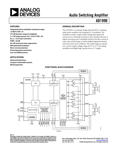
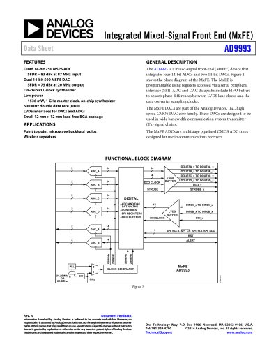
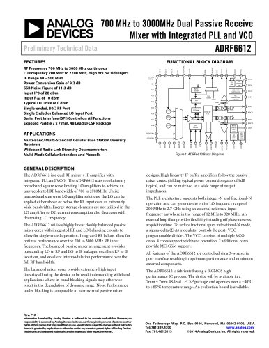
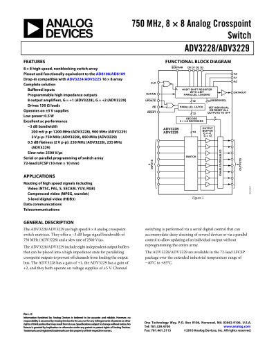
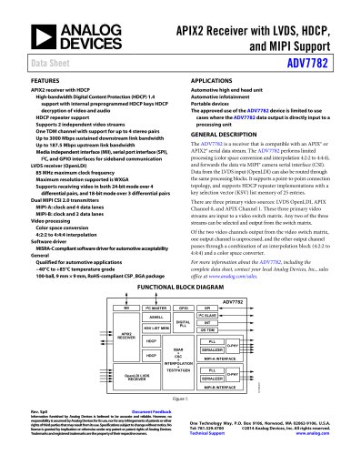
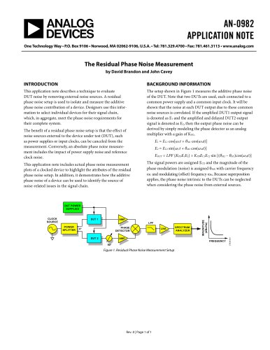
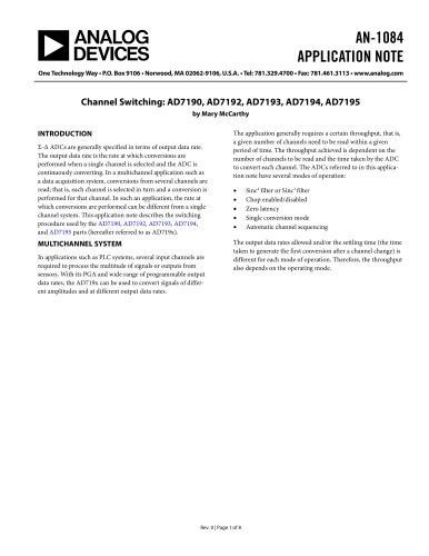
FUNCTIONAL BLOCK DIAGRAM
REF = 2.5V TO 5V
2.5V
0V TO VREF
IN1+
ADC1
IN1–
0V TO VREF
IN2+
ADC2
IN2–
GND
VDD1 VDD2
VIO1
VIO1/VIO2
SDI1
SDI1/SDI2
SCK1
SCK1/SCK2
CNV1
CNV1/CNV2
SDO1
SDO1
VIO2
SDI2
SCK2
CNV2
SDO2
AD7902
3-WIRE OR 4-WIRE
INTERFACE
(SPI, CS, AND
CHAIN MODES)
SDO2
11756-001
REF1 REF2
Figure 1.
Rev. 0
Document Feedback
Information furnished by Analog Devices is believed to be accurate and reliable. However, no
responsibility is assumed by Analog Devices for its use, nor for any infringements of patents or other
rights of third parties that may result from its use. Specifications subject to change without notice. No
license is granted by implication or otherwise under any patent or patent rights of Analog Devices.
Trademarks and registered trademarks are the property of their respective owners.
One Technology Way, P.O. Box 9106, Norwood, MA 02062-9106, U.S.A.
Tel: 781.329.4700
©2014 Analog Devices, Inc. All rights reserved.
Technical Support
www.analog.com