عضویت
عضویت  ورود اعضا
 راهنمای خرید


AD5623R/AD5643R/AD5663R: Dual 12-/14-/16-Bit nanoDAC® with 5 ppm/°C On-Chip0 pages
Dual 12-/14-/16-Bit nanoDAC® with
5 ppm/°C On-Chip Reference
AD5623R/AD5643R/AD5663R
Data Sheet
FEATURES
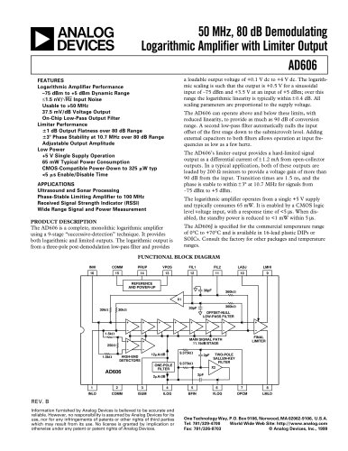
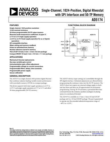
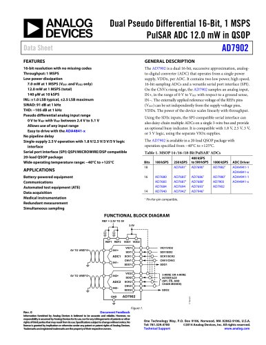
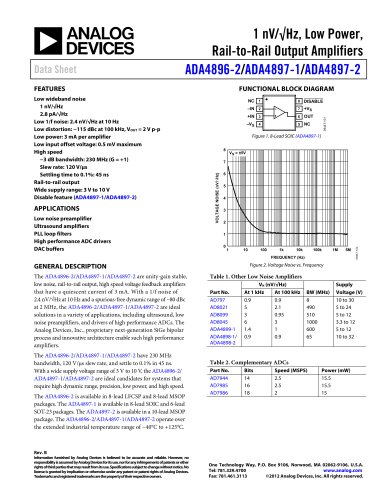
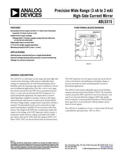
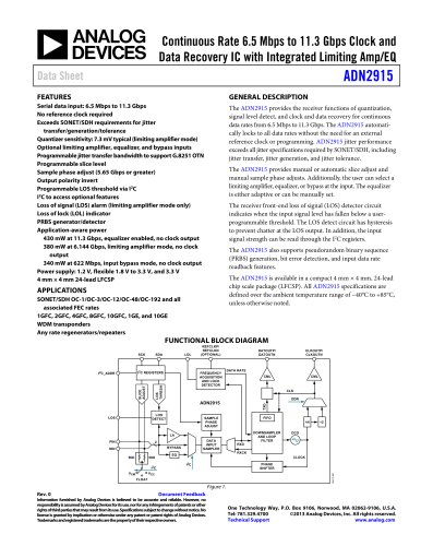
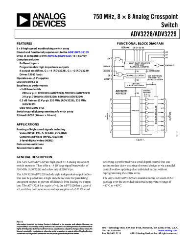
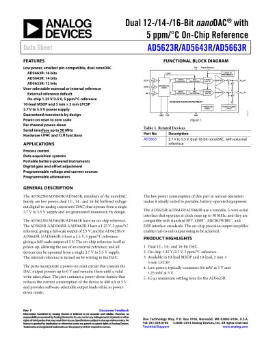
FUNCTIONAL BLOCK DIAGRAM
APPLICATIONS
VDD
VREFIN /VREFOUT
1.25V/2.5V
REFERENCE
LDAC
INPUT
REGISTER
SYNC
DAC
REGISTER
STRING
DAC A
BUFFER
VOUTA
INPUT
REGISTER
SCLK
DAC
REGISTER
STRING
DAC B
BUFFER
VOUTB
INTERFACE
LOGIC
DIN
AD5623R/AD5643R/AD5663R
POWER-ON
RESET
POWER-DOWN
LOGIC
GND
LDAC CLR
05858-001
Low power, smallest pin-compatible, dual nanoDAC
AD5663R: 16 bits
AD5643R: 14 bits
AD5623R: 12 bits
User-selectable external or internal reference
External reference default
On-chip 1.25 V/2.5 V, 5 ppm/°C reference
10-lead MSOP and 3 mm × 3 mm LFCSP
2.7 V to 5.5 V power supply
Guaranteed monotonic by design
Power-on reset to zero scale
Per channel power-down
Serial interface up to 50 MHz
Hardware LDAC and CLR functions
Figure 1.
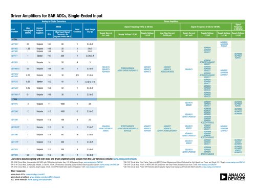
Table 1. Related Devices
Part No.
AD5663
Description
2.7 V to 5.5 V, dual 16-bit nanoDAC, with external
reference
Process control
Data acquisition systems
Portable battery-powered instruments
Digital gain and offset adjustment
Programmable voltage and current sources
Programmable attenuators
GENERAL DESCRIPTION
The AD5623R/AD5643R/AD5663R, members of the nanoDAC
family, are low power, dual 12-, 14-, and 16-bit buffered voltageout digital-to-analog converters (DAC) that operate from a single
2.7 V to 5.5 V supply and are guaranteed monotonic by design.
The AD5623R/AD5643R/AD5663R have an on-chip reference.
The AD5623R-3/AD5643R-3/AD5663R-3 have a 1.25 V, 5 ppm/°C
reference, giving a full-scale output of 2.5 V; and the AD5623R-5/
AD5643R-5/AD5663R-5 have a 2.5 V, 5 ppm/°C reference,
giving a full-scale output of 5 V. The on-chip reference is off at
power-up, allowing the use of an external reference; and all
devices can be operated from a single 2.7 V to 5.5 V supply.
The internal reference is turned on by writing to the DAC.
The parts incorporate a power-on reset circuit that ensures the
DAC output powers up to 0 V and remains there until a valid
write takes place. The part contains a power-down feature that
reduces the current consumption of the device to 480 nA at 5 V
and provides software-selectable output loads while in powerdown mode.
Rev. F
The low power consumption of this part in normal operation
makes it ideally suited to portable, battery-operated equipment.
The AD5623R/AD5643R/AD5663R use a versatile, 3-wire serial
interface that operates at clock rates up to 50 MHz, and they are
compatible with standard SPI®, QSPI™, MICROWIRE™, and
DSP interface standards. The on-chip precision output amplifier
enables rail-to-rail output swing to be achieved.
PRODUCT HIGHLIGHTS
1. Dual 12-, 14-, and 16-bit DAC.
2. On-chip 1.25 V/2.5 V, 5 ppm/°C reference.
3. Available in 10-lead MSOP and 10-lead, 3 mm ×
3 mm LFCSP.
4. Low power; typically consumes 0.6 mW at 3 V and
1.25 mW at 5 V.
5. 4.5 μs maximum settling time for the AD5623R.
Document Feedback
Information furnished by Analog Devices is believed to be accurate and reliable. However, no
responsibility is assumed by Analog Devices for its use, nor for any infringements of patents or other
rights of third parties that may result from its use. Specifications subject to change without notice. No
license is granted by implication or otherwise under any patent or patent rights of Analog Devices.
Trademarks and registered trademarks are the property of their respective owners.
One Technology Way, P.O. Box 9106, Norwood, MA 02062-9106, U.S.A.
Tel: 781.329.4700 ©2006–2013 Analog Devices, Inc. All rights reserved.
Technical Support
www.analog.com