عضویت
عضویت  ورود اعضا
 راهنمای خرید


ADN2525: 10.7 Gbps Active Back-Termination, Differential Laser Diode Driver 0 pages
10.7 Gbps Active Back-Termination,
Differential Laser Diode Driver
ADN2525
Rev. A
Information furnished by Analog Devices is believed to be accurate and reliable. However, no
responsibility is assumed by Analog Devices for its use, nor for any infringements of patents or other
rights of third parties that may result from its use. Specifications subject to change without notice. No
license is granted by implication or otherwise under any patent or patent rights of Analog Devices.
Trademarks and registered trademarks are the property of their respective owners.
One Technology Way, P.O. Box 9106, Norwood, MA 02062-9106, U.S.A.
Tel: 781.329.4700 www.analog.com
Fax: 781.461.3113 ©2006 Analog Devices, Inc. All rights reserved.
FEATURES
Up to 10.7 Gbps operation
Very low power: 670 mW (IBIAS = 40 mA, IMOD = 40 mA)
Typical 24 ps rise/fall times
Full back-termination of output transmission lines
Compatible with XMD-MSA TOSA
Drives TOSAs with resistances ranging from 5 Ù to 50 Ù
PECL-/CML-compatible data inputs
Bias current range: 10 mA to 100 mA
Differential modulation current range: 10 mA to 80 mA
Automatic laser shutdown (ALS)
3.3 V operation
Compact 3 mm × 3 mm LFCSP
Voltage input control for bias and modulation currents
XFP-compliant bias current monitor
Optical evaluation board available
APPLICATIONS
SONET OC-192 optical transceivers
SDH STM-64 optical transceivers
10 Gb Ethernet optical transceivers
XFP/X2/XENPAK/XPAK/MSA 300 optical modules
SR and VSR optical links
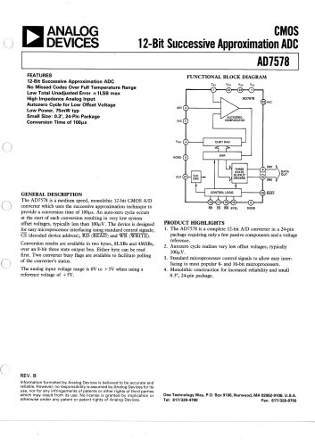
GENERAL DESCRIPTION
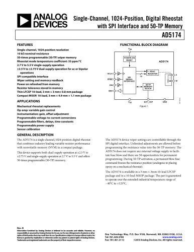
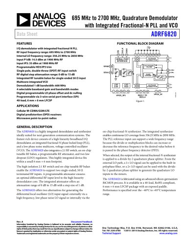
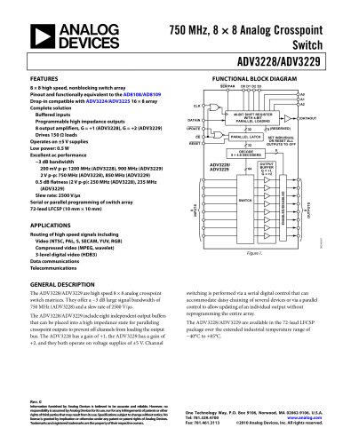
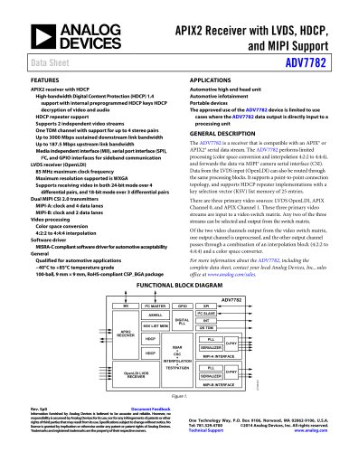
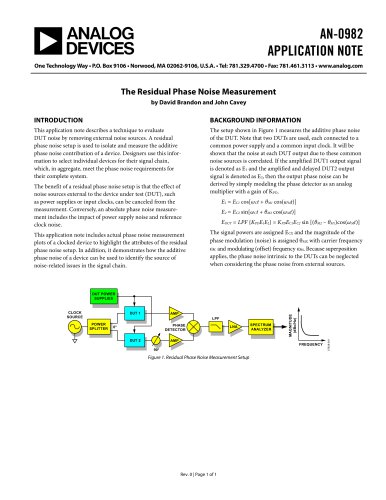
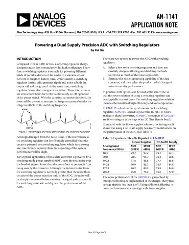
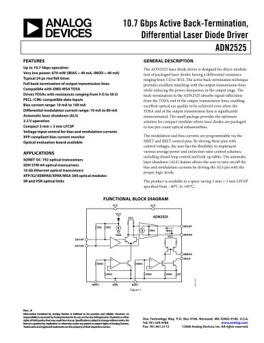
The ADN2525 laser diode driver is designed for direct modula-tion of packaged laser diodes having a differential resistance ranging from 5 Ù to 50 Ù. The active back-termination technique provides excellent matching with the output transmission lines while reducing the power dissipation in the output stage. The back-termination in the ADN2525 absorbs signal reflections from the TOSA end of the output transmission lines, enabling excellent optical eye quality to be achieved even when the TOSA end of the output transmission lines is significantly misterminated. The small package provides the optimum solution for compact modules where laser diodes are packaged in low pin-count optical subassemblies.
The modulation and bias currents are programmable via the MSET and BSET control pins. By driving these pins with control voltages, the user has the flexibility to implement various average power and extinction ratio control schemes, including closed-loop control and look-up tables. The automatic laser shutdown (ALS) feature allows the user to turn on/off the bias and modulation currents by driving the ALS pin with the proper logic levels.
The product is available in a space-saving 3 mm × 3 mm LFCSP specified from -40°C to +85°C.
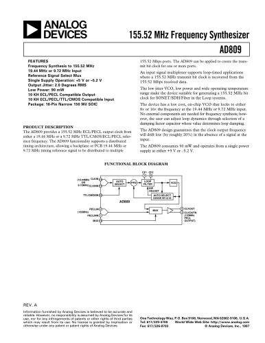
FUNCTIONAL BLOCK DIAGRAM 50Ù200Ù800Ù200Ù2ÙVCCDATAPDATANMSETGNDBSETIBMONIBIASIMODPIMODNADN2525VCCALSGNDVCCVCC50Ù50Ù200Ù800ÙIMOD05077-001
Figure 1.