عضویت
عضویت  ورود اعضا
 راهنمای خرید


ADP2230: Dual 2 MHz, 800 mA, Synchronous, Low Quiescent Current Buck Regulator Data Sheet0 pages
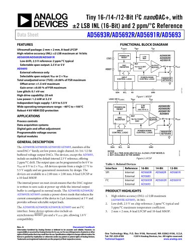
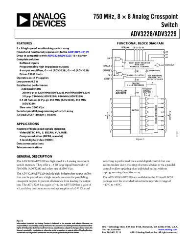
FEATURES
TYPICAL APPLICATION CIRCUIT
Input voltage range: 2.3 V to 6.5 V
Fixed and adjustable output voltage options
Fixed output voltage pair options: 1.2 V/1.8 V, 1.2 V/3.3 V,
1.8 V/3.3 V
Adjustable output voltage range: 0.8 V to 6 V
Minimum guaranteed continuous output current: 800 mA
Up to 94% efficiency
Low quiescent current of 15 µA for both channels in power
saving mode (PSM)
Low shutdown current: 0.1 μA (typical)
100% duty cycle for low dropout operation
SYNC pin switching frequency options
2 MHz fixed pulse-width modulation (PWM) mode
2 MHz PSM/PWM automatic transitioning mode
External clock synchronization from 1.5 MHz to 2.5 MHz
Enable input with precision thresholds for each output
180° phase shifted PWM outputs for minimum VIN ripple
Current-limit and thermal shutdown (TSD) protection
Quick output discharge (QOD)
10-lead, 3 mm × 3 mm × 0.75 mm LFCSP package
APPLICATIONS
Portable and battery-powered equipment
Automatic meter readers (WSN)
Point of sales and transaction processing instruments
Mobile phones
Digital cameras and audio devices
Medical instruments
Medium format display tablets and pads
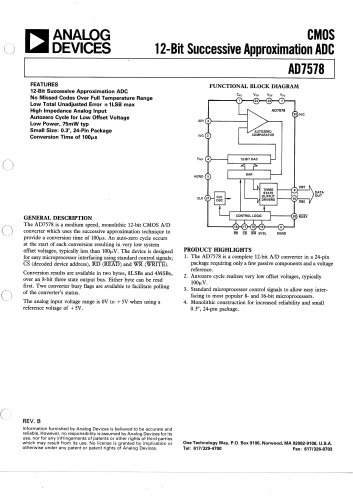
GENERAL DESCRIPTION
The ADP2230 includes two high efficiency, low quiescent current,
800 mA, step-down, dc-to-dc converters in a small, 10-lead,
3 mm × 3 mm, LFCSP package. The total solution requires only
five tiny external components. When the ADP2230 is used with
three 0603 capacitors and two 2 mm × 2 mm inductors, the
total solution size is about 48 mm2, resulting in the smallest
footprint solution to meet a variety of portable applications.
The ADP2230 buck regulator uses a proprietary, high speed,
current mode, constant frequency, PWM control scheme for
excellent stability and transient response. The buck outputs
operate out of phase to reduce the input current ripple.
To ensure the longest battery life in portable applications, the
ADP2230 has a power saving variable frequency mode that
reduces the switching frequency under light load conditions.
Rev. 0
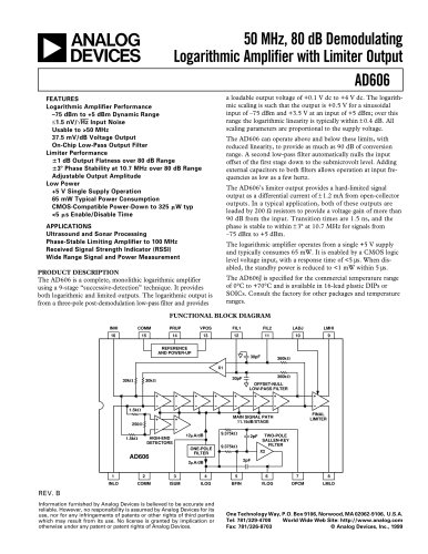
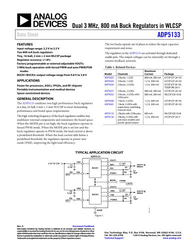
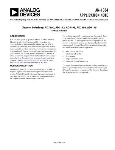
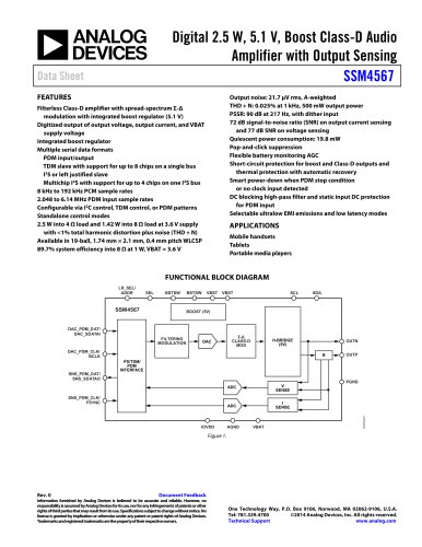
ADP2230
VIN
2
9
CIN
10µF
VIN1
L1
2.2µH
VIN2
VOUT1
SW1 1
COUT1
10µF
FB1 3
ON
ON
OFF
4
EN1
7
EN2
6
OFF
SYNC
L2
2.2µH
SW2 10
VOUT2
PWM
FB2 8
AGND
PGND
(EPAD)
5
11
PSM/PWM
COUT2
10µF
10705-001
Data Sheet
Dual 2 MHz, 800 mA, Synchronous, Low
Quiescent Current Buck Regulator
ADP2230
Figure 1. Fixed Output Voltage Typical Application Circuit
During logic controlled shutdown, the input is disconnected
from the output, and it draws less than 0.1 μA from the input
source. The ADP2230 operates from input voltages from 2.3 V
to 6.5 V, allowing the use of multiple alkaline, NiMH, or lithium
cells and other standard power sources.
The ADP2230 offers multiple options for setting the operating
frequency. To maximize light load efficiency, the ADP2230 can
operate at a reduced switching frequency in PSM and switch
automatically to PWM as the load increases. The ADP2230 can
be forced to operate at 2 MHz in PWM only mode when noise
considerations are more important than efficiency. The
ADP2230 can also be synchronized with a 1.5 MHz to 2.5 MHz
external clock via the SYNC pin. When using the external clock
synchronization control, both buck outputs operate in phase
with the applied clock signal.
The ADP2230 includes an internal power switch, synchronous
rectifier, and compensation to minimize external part count
and maximize efficiency. Other key protection features include
undervoltage lockout to prevent deep battery discharge, internal
soft start to prevent input current overshoot at startup, and an
integrated, switched resistor, QOD function that automatically
discharges the output when the device is disabled. Short-circuit
protection and thermal overload protection circuits prevent
damage in adverse conditions.
Document Feedback
Information furnished by Analog Devices is believed to be accurate and reliable. However, no
responsibility is assumed by Analog Devices for its use, nor for any infringements of patents or other
rights of third parties that may result from its use. Specifications subject to change without notice. No
license is granted by implication or otherwise under any patent or patent rights of Analog Devices.
Trademarks and registered trademarks are the property of their respective owners.
One Technology Way, P.O. Box 9106, Norwood, MA 02062-9106, U.S.A.
Tel: 781.329.4700
©2014 Analog Devices, Inc. All rights reserved.
Technical Support
www.analog.com