عضویت
عضویت  ورود اعضا
 راهنمای خرید


PCI Express Dual SGDMA system for Cyclone IV0 pages
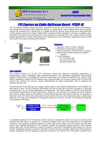
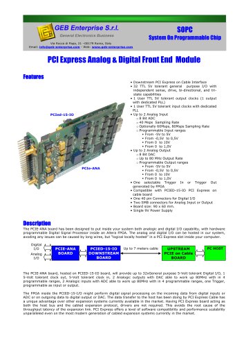
SOPC
System On Programmable Chip
Via Rocca di Papa, 21 –00179 Roma, Italy
Email: info@geb-enterprise.com - Web: www.geb-enterprise.com
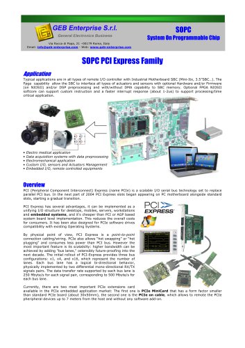
SOPC PCIe System: Dual High Speed SGDMA
Overview
PCI Express family systems are a set of typical basic systems targeted on GEB PCIe boards family (Cyclone IV
GX Fpga) which contains all files to make a PCIe subsystem quickly: Configuration files to load on fpga, sopc
files, related drivers for multiple OS, simple Demo and test programs. All support files are available in source
format. Customer can use the basic system to develops his application hardware and software directly on GEB
board, which can be sold in volume at low cost, or may retarget his application on his hardware editing the
source files.
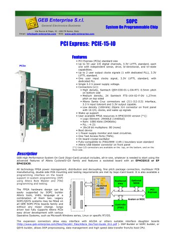
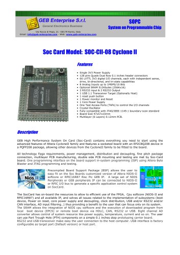
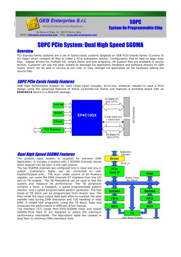
SOPC PCIe Cards Family Features
GEB High Performance System On Card (Sopc-Card) includes, all-in-one, whatever needed to start a PCIe
design using the advanced features of Altera CycloneIV-GX family and features a socketed board with an
EP4CGX15 device in a BGA169 package.
33 digital I/O
3V3 LVTTL
Reset
EP4C15GX
Clock
I/O Connectors
1V2 PS
2 user clock out
1 clock input
PCI Express.
20 digital I/O
3V3 LVTTL
Application
Interface
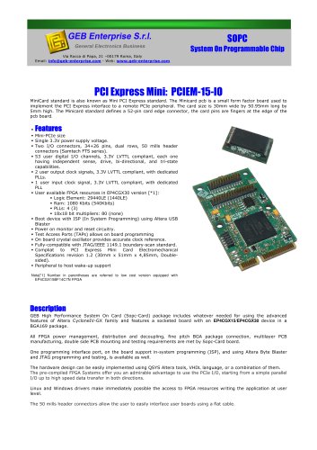
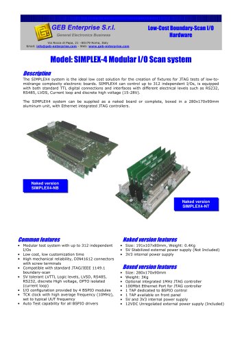
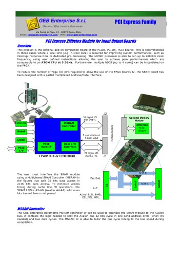
Dual High Speed SGDMA Features
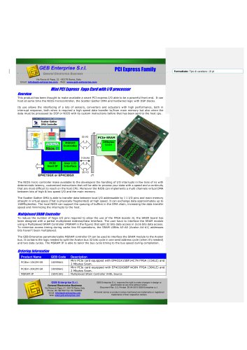
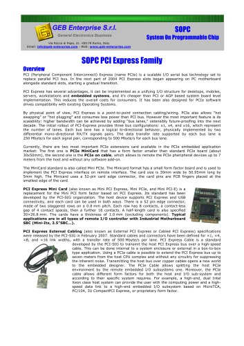
The present basic system is targeted for extreme DMA
Application. It includes a system with 2 SGDMA channels whose
block diagram can be seen in the right picture.
The two SGDMA channels are configured one in input and one
in output. Customer's logics can be connected to user
Inputs/Outputs pins. The mux, under control of an Avalon’s
register, can route the DMA channels ST interface from the I/O
pins to TB module. The TB Pheripheral can be used to test the
system and measure its performance. The TB peripheral
contains a timer, a loopback, a speed programmable pattern
checker, and a speed programmable pattern generator. The
test mode of TB block can be programmed from Avalon bus.
The fifos inside the input output data path allow to mantain the
data transfer rate during DMA descriptor and TLB handling in
wide DMA. A simple test programm, using the TB block, tests
and measures the performance in different driver layouts.
The interface (ST) inside MUX-FIFO-SGDMA chain and iniside
SGDMA-PCIe Hard IP are designed to obtain the maximum
performance reacheable. The descriptors table are created in
local Ram to minimize DMA interblock time.
Driver
PCIE x1
PCIe
Hard IP
RAM
Avalon Cross
Bar Switch
SGDMA
SGDMA
FIFO
FIFO
MUX
MUX
TB
User Inputs Outputs