عضویت
عضویت  ورود اعضا
 راهنمای خرید


Vme Bus Rapid Development Kit0 pages
VME SOPC
s
System On Programmable Chip
Via Rocca di Papa, 21 –00179 Roma, Italy
Email: info@geb-enterprise.com - Web: www.geb-enterprise.com
VME BUS Family
Overview
The VME Bus family has the target to make available at low cost the resources to build a fast prototype of a
VME master/slave/controller subsytem. The modularity of the resources, both hardware board and firmware
VHDL IP allow to compose many types of application with a low effort.
The application field may be:
•
In heterogeneous systems, when you wish to make a soft growth up, a mixture of different form factor
boards and a flexible bridge could
be needed, for instance beetween PC/PXI bus and VME
standard/customized bus.
•
In components or boards obsolescence replacement.
•
In test systems to perform test cycles to UUT slave board and/or to acknowledge bus cycles from an
UUT master board and to perform bus signals check at some time.
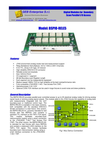
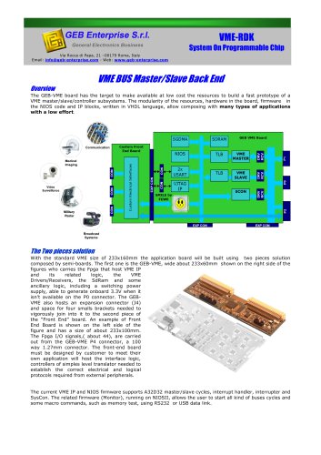
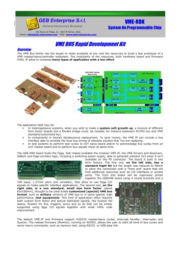
GEB VME Family
Main Parts
GEB VME Board
SGDMA
SDRAM
VJTAG
IP
TLB
VME
MASTER
TLB
VME
SLAVE
P1
P0
DRV
RCV
P2
BRIDGE
EXP CON
EXP CON
BUS
Sniffer
PCIe
cabled
PCIEd Board
DRV
RCV
USB2
DRV
RCV
NIOS
SCON
EXP CON
CON
2x
USART
DRV
RCV
CON
EXP CON
CON
CON
Santa
Crutz
Slot
CON
2x
RS232
CON
FE Board
1149.1
TAPs
VANA Board
The GEB-VME board hosts the Fpga, that makes available the modular VME IP, the VME Drivers and Receivers,
SdRam and Fpga ancillary logic, including a switching power supply, able to generate onboard 3V3 when it isn’t
available on the P0 connector. The board is built in two form
factors. The first one, on the left side, has a standard hight 6U
but the length was reduced to 58mm to allow the connection
with a “front end” board that will host additional resources such
as I/O interfaces or access ports. The front end board will be
vigorously joined together the GEBVME board using 4 smalls
brackets and a 100 ways, 1.27mm pitch smt connettor, that allow to use
Fpga I/O signals to make specific interface applications. The second one, on
the right side, is a non standard, small size form factor (about 83x108mm),
thought to be used inside customized (special) VME bus format, such as
Avionic or Naval versions of VME bus or in some special, high performance,
test equipments. This kind of application often requires both custom form
factor and special dedicated signals, like System fail status, System On line,
triggers, syncs and so on that can be simply supported using fpga I/O
signals together with small VHDL code improvement.
The default VME-IP and firmware support A32D32 master/slave cycles, interrupt handler, interrupter and
SysCon. The related firmware (Monitor), running on NIOSII, allows the user to start all kind of bus cycles and
some macro commands, such as memory test, using RS232 or USB data link.