عضویت
عضویت  ورود اعضا
 راهنمای خرید


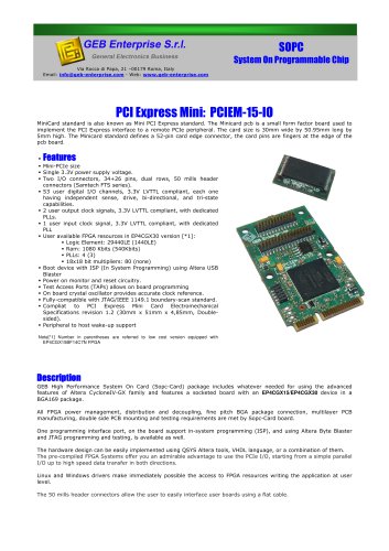
SRAM add-on for PCIe Fpga cards family0 pages
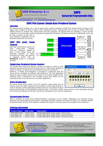
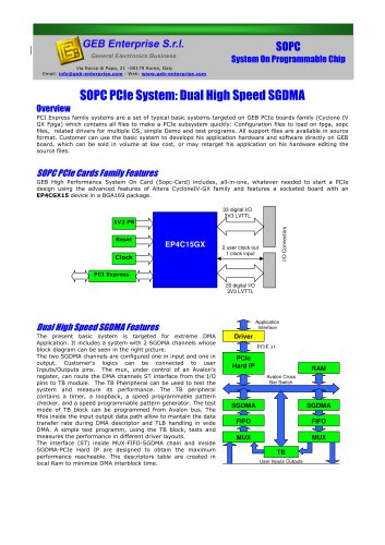
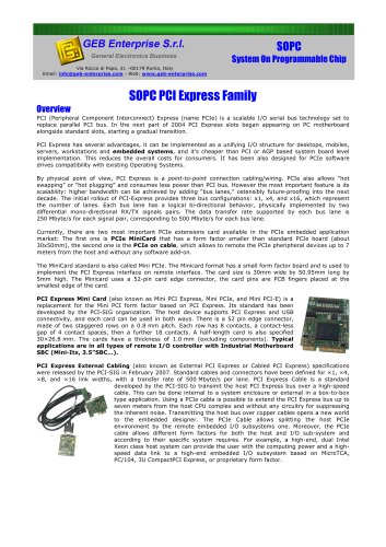
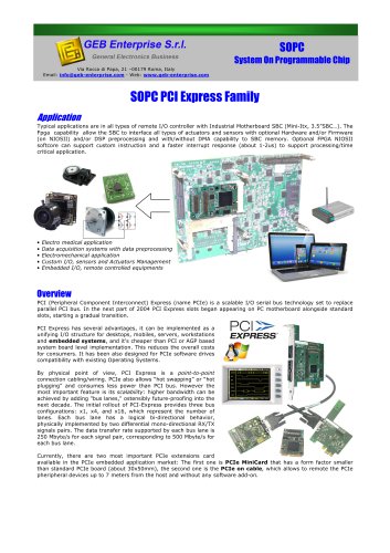
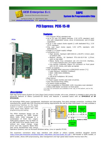
PCI Express Family
Via Rocca di Papa, 21 –00179 Roma, Italy
Email: info@geb-enterprise.com - Web: www.geb-enterprise.com
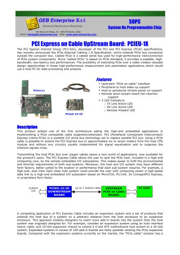
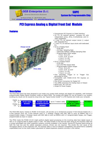
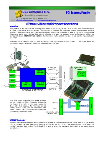
PCI Express 2Mbytes Module for Input Output Boards
Overview
This product is the optional add-on companion board of the PCIed, PCIem, PCIe boards. This is recommended
in those cases where a local CPU (e.g. NIOSII core) is required for improving system performances, such as
interrupt response time or dedicated pre-processing. The NIOSII processor is able to run up to 200MHz clock
frequency, using user defined instructions allowing the user to achieve peak performances which are
comparable to an ATOM CPU at 3.2GHz. Furthermore, multiple NIOS (up to 4 cores) can be instantiated on
the FPGA.
To reduce the number of Fpga I/O pins required to allow the use of the FPGA boards J2, the SRAM board has
been designed with a partial multiplexed Address/Data Interface.
J2
33 digital I/O
3V3 LVTTL
I/O Connectors
MSRAM
Controller
Reset
2 user clock out
1 clock input
Clock
User I/O
Interface
EP4C15GX or EP4C30GX
20 digital I/O
3V3 LVTTL
The user must interface the SRAM module
using a Multiplexed SRAM Controller (MSRAM in
DA(19-4)
the figure) that split 32 bits data access in
2x16 bits data access. To minimize access
timing during cache line fill operations, the
ALE
SRAM LSBits A3-A0 (Avalon A4-A1) addresses
bits haven’t been multiplexed.
A(3-0), BLEL, BHEL,
J1
D(15-0)
A(19-4)
SRAM
PCIE
Hard IP
J2
PCIe
I/F
2Mbytes
PCIeSRAM
Latch
1V2 PS
Optional Memory
Module
CEL,RDL, WRL,
MSRAM Controller
The GEB Enterprise parametric MSRAM controller IP can be used to interface the SRAM module to the Avalon
bus. It contains the logic needed to split the Avalon bus 32 bits cycle in one send address cycle (when it’s
needed) and two data cycles. The MSRAM IP is able to tailor the bus cycle timing to the bus speed during
compilation.