عضویت
عضویت  ورود اعضا
 راهنمای خرید


S6BP501A , S6BP502A 3ch DC/DC Converter IC for Automotive Cluster0 pages
S6BP501A, S6BP502A
PRELIMINARY
3ch DC/DC Converter IC
for Automotive Cluster
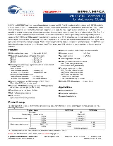
S6BP501A/S6BP502A is a three channel output power management IC. This IC includes one high voltage buck DC/DC controller
(DD3V), one buck DC/DC converter with built-in FETs (DD1V) and one boost DC/DC converter with built-in FETs (DD5V). Current
mode architecture is used for fast load transient response. At no load, the input supply current is reduced to 15 µA (Typ). It is
possible to provide stable output voltage under an automotive cold cranking condition until the input voltage falls to 2.5V. This IC is
suitable for power supply solutions of automotive and Industrial applications. Each output voltage can be adjusted by external
resistors. Both DD1V and DD5V support the switching frequencies up to 2.4 MHz to allow use of small size inductors, which can
reduce a part mounting area. To decrease EMI, this IC equips a SYNC function that synchronizes to an external clock signal and a
spread spectrum clock generator (SSCG). When not inputting an external clock, it operates by an internal clock. The SSCG is valid
both internal clock and external clock. Moreover, this IC has power good (PG) monitors for each output and a thermal-warning
indicator.
Features
Wide input voltage range
Synchronous rectification current mode architecture
: 2.5V to 42V (DD3V)
Adjustable output voltage with pairs of resistors
DD1V
DD3V
DD5V
: 1.0V to 1.3V
: 3.2V to 3.4V
: 5.0V to 5.2V
Shutdown current
: 1 µA (Typ)
Quiescent current
: 15 µA (Typ)
Load-independent soft-start
Power good monitors for each output
OVD
Switching frequency range (synchronizable to external clock
by SYNC function)
DD1V, DD5V
Internal clock operation
: 2.1 MHz (Typ)
External clock operation
: 1.8 MHz to 2.4 MHz
DD3V (one-fifth-divided clock)
Internal clock operation
: 420 kHz (Typ)
External clock operation
: 360 kHz to 480 kHz
Super-high efficiency by PFM operation (DD3V, DD5V :
UVD
(over voltage detection)
(under voltage detection)
Enhanced protection functions
UVLO
(under voltage lockout)
(over voltage protection)
OCP (over current protection)
TSD (thermal shutdown)
TWI (thermal warning indicator)
OVP
Wettable QFN-32 package
: 5 mm × 5 mm
When fixing SYNC pin to a low level)
Automatic PWM/PFM switching and fixed PWM operations
are settable by SYNC pin (DD3V, DD5V)
Applications
Operable on up to 100% duty (DD3V)
Instrument cluster
Built-in phase compensators
Automotive applications
Built-in SSCG
Industrial applications
(spread spectrum clock generator)
Product Lineup
To order a product, select an item from the product lineup blow. For information on the ordering part number, please see "13.
Ordering Information".
Product Name
S6BP501A
S6BP502A
Pin count
32
Power supply voltage range
2.5V to 42V
DD1V
1.0V to 1.3V
Output voltage range
DD3V
3.2V to 3.4V
DD5V
5.0V to 5.2V
DD1V
1.4A
2.0A
Maximum output current
SW3V (*1)
1.6A
1.9A
DD5V
1.3A
1.3A
Package
QFN-32 (VNG032)
*1: Load switch for DD3V. Each value is the maximum output current via SW3V.
Errata: For information on silicon errata, see “15. Errata" on page 22.
Cypress Semiconductor Corporation
Document Number: 002-03396 Rev.*B
•
198 Champion Court
•
"