عضویت
عضویت  ورود اعضا
 راهنمای خرید


S25FS064S 64 Mbit (8 Mbyte) 1.8 V FS S Flash Memory0 pages
ADVANCE
S25FS064S
64 Mbit (8 Mbyte)
1.8-V FS-S Flash Memory
Features
Serial Peripheral Interface (SPI) with Multi-I/O
– SPI Clock polarity and phase modes 0 and 3
– Double Data Rate (DDR) option
– Extended Addressing - 24 or 32-bit address options
– Serial Command subset and footprint compatible with S25FL1-K,
S25FL-P and S25FL-S SPI families
– Multi I/O Command subset & footprint compatible with S25FL1-K
S25FL-P and S25FL-S SPI families
Read
– Commands: Normal, Fast, Dual Output, Dual I/O, Quad Output,
Quad I/O, DDR Quad I/O
– Modes: Burst Wrap, Continuous (XIP), QPI (QPI)
– Serial Flash Discoverable Parameters (SFDP) and Common Flash
Interface (CFI), for configuration information.
Program
– 256 or 512 Bytes Page Programming buffer
– Program suspend and resume
Erase
– Hybrid sector option
– Physical set of eight 4KB sectors and one 32KB sector at the top
or bottom of address space with all remaining sectors of 64KB
– Uniform sector option
Security features
– One Time Program (OTP) array of 1024 bytes
– Block Protection:
– Status Register bits to control protection against program or erase
of a contiguous range of sectors.
– Hardware and software control options
– Advanced Sector Protection (ASP)
– Individual sector protection controlled by boot code or password
– Option for password control of read access
Technology
– Cypress 65 nm MirrorBit® Technology with Eclipse Architecture
Single Supply Voltage with CMOS I/O
– 1.7V to 2.0V
Temperature Range
– Industrial (40°C to +85°C)
– Industrial Plus (40°C to +105°C)
– Extended (40°C to +125°C)
Packages (all Pb-free)
– 8-lead SOIC 208 mil (SOC008)
– BGA-24 6 8 mm
– 5 5 ball (FAB024) footprint
– Known Good Die and Known Tested Die
– Uniform 64KB or 256KB blocks for software compatibility with
higher density and future devices
–
–
–
–
Erase suspend and resume
Erase status evaluation
100,000 Program-Erase Cycles on any sector, minimum
20 Year Data Retention, typical
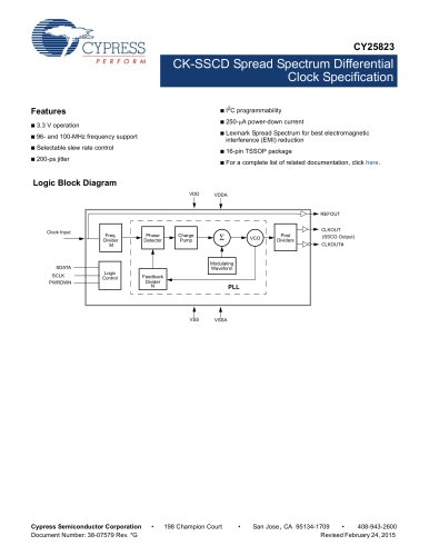
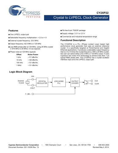
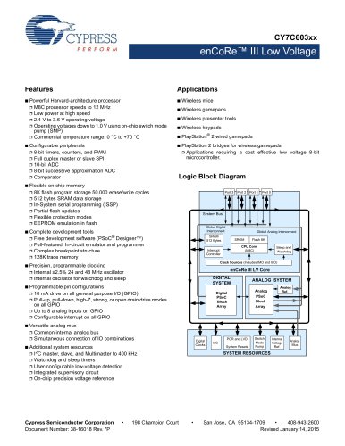
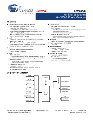
Logic Block Diagram
CS#
X Decoders
SRAM
SCK
SI/IO0
SO/IO1
MirrorBit Array
Y Decoders
I/O
Data Latch
WP#/IO2
Control
Logic
RESET#/IO3
Data Path
RESET#
Cypress Semiconductor Corporation
Document Number: 002-0363