عضویت
عضویت  ورود اعضا
 راهنمای خرید


CTLTVS120 pages
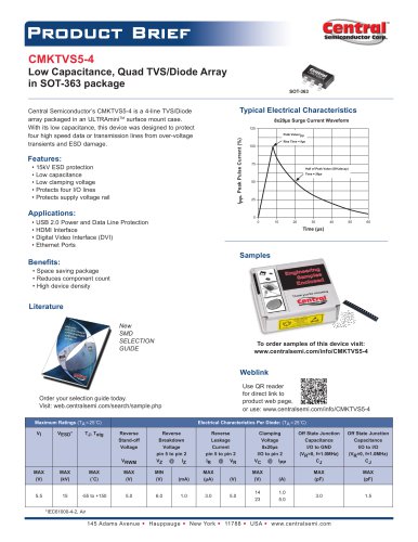
PRODUCT BRIEF
CTLTVS12
Transient Voltage Suppressor
in the miniature TLM2D3D6 package
Central
Semiconductor Corp.
TLM2D3D6
package
Top View Bottom View
Central Semiconductor's CTLTVS12 is a space saving, low
leakage TVS in the ultra small, ultra low profile TLM2D3D6
surface mount package. This device is designed to protect
sensitive equipment against ESD damage.
Features:
• Ultra small, ultra low profile package
• Low capacitance
• Low leakage current
• ESD protection IEC 61000-4-2:
Air discharge - 30kV
Contact discharge - 30kV
Applications:
• Data line / User interface protection
• DC power rail clamping
• ESD protection of logic level ICs
Benefits:
• Low idle power consumption
• Low profile
• Space saving
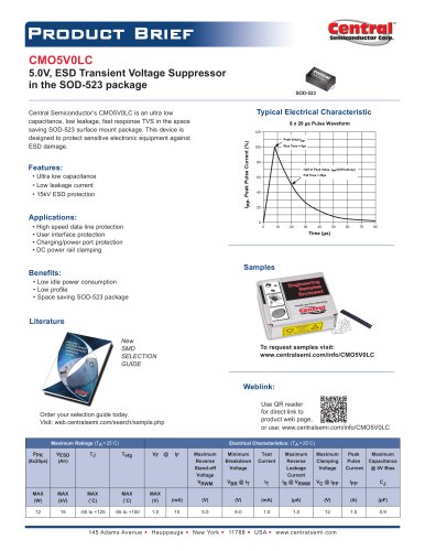
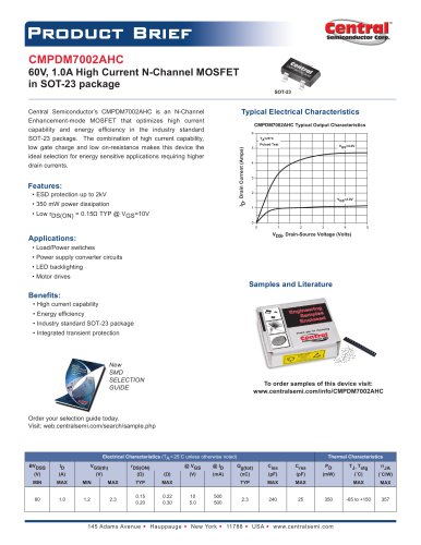
Typical Electrical Characteristics
8 x 20 us Pulse Waveform
U
a
«
D.
Q
a.
-0" 20
I I | ||||
— Peak Value lpp - RIs* Tlma ■ Bus | ||||
Fall Time = 20ua | ||||
0 10 20 30 40 50 60 70
Time (us)
Samples
Literature
New
SMD
SELECTION
GUIDE
To order samples of this device visit:
www.centralsemi.com/info/CTLTVS12
Order your selection guide today.
Visit: web.centralsemi.com/search/sample.php
Use QR reader
for direct link to
product web page.
weblink scan
m
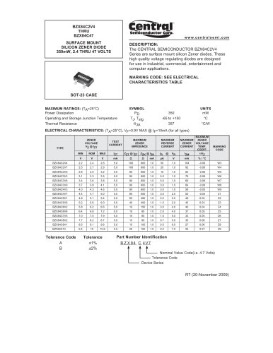
Maximum Ratings (T^ = 25"C)
Electrical Characteristics: (T^ = 25"C)
PPK | VESD | Tj, Tstg | vF @ iF | Maximum Reverse Stand-off Voltage VRWM | Breakdown Voltage VBR @ lT | Test Current IT | Maximum Reverse Leakage Current IR @ VRWM | Maximum Clamping Voltage Vc @ lpp | Peak Pulse Current lpp | Typical Capacitance @ 0V Bias | Typical Capacitance @ 9V Bias | |||
MAX (W) | MAX (kV) | MAX CC) | MAX (V) | (mA) | (V) | MIN (V) | NOM (V) | MAX (V) | (mA) | (UA) | (V) | (A) | (PF) | (PF) |
35 | 30 | -55 to+150 | 1.0 | 10 | 9.0 | 10 | 12 | 14 | 5.0 | 1.0 | 18 | 1.8 | 14 | 5.0 |
145 Adams Avenue • Hauppauge • New York • 11788 * USA* www.centralsemi.com
"