عضویت
عضویت  ورود اعضا
 راهنمای خرید
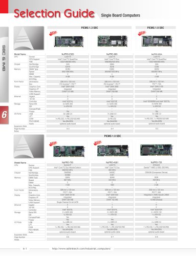
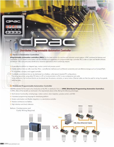


PCI-9114 Series0 pages
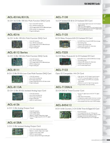
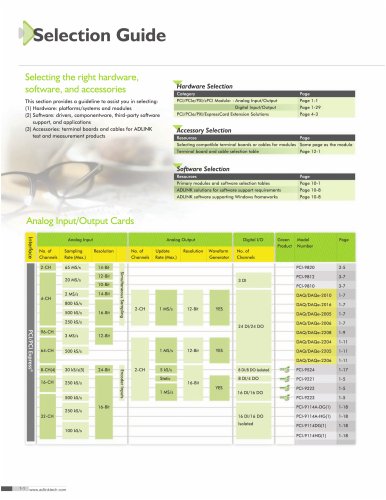
General-Purpose DAQ
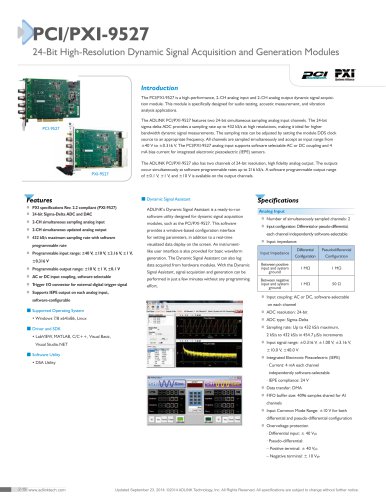
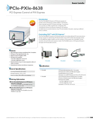
PCI-9114 Series
32-CH 16-Bit Up to 250 kS/s Multi-Function DAQ Cards
Specifications
Analog Input
t ■t Number of channels: 32 single-ended or 16 differential
t ■t Resolution: 16 Bit
t ■t Conversion time:
tt · 10 μs (PCI-9114DG)
tt · 4 μs (PCI-9114A-DG & PCI-9114A-HG)
t ■t Maximum sampling rate
t
Device
Sampling rate
PCI-9114DG
Features
Supports a 32-Bit 5 V PCI bus
■t 16-Bit A/D resolution
■t Up to 100 kS/s sampling rate (PCI-9114DG)
■t Up to 250 kS/s sampling rate (PCI-9114A-DG and
tPCI-9114A-HG)
■t 32-CH single-ended or 16-CH differential analog inputs
■t Bipolar or unipolar analog input ranges
■t Onboard 1 k-sample A/D FIFO
■t Programmable gains:
t • x1, x2, x4, x8 (PCI-9114DG and PCI-9114A-DG)
t • x1, x10, x100 (PCI-9114A-HG)
■t Automatic analog inputs scanning
■t 16-CH isolated digital inputs and 16-CH isolated digital outputs
■t 2500 VRMS optical isolation for digital inputs and outputs
■t 1-CH 16-Bit general-purpose timer/counter
■t +12 V and -12 V power available on the 37-pin D-sub connector
■t Onboard resettable fuses for power output protection
■t Compact, half-size PCB
t ■t
■t
■tSupported Operating System
t
• Windows 7/8 x64/x86, Linux
■tDriver and SDK
t
• LabVIEW, MATLAB, C/C++, Visual Basic,
Visual Studio.NET
■tSoftware Utility
t
• AD-Logger
100 kS/s
PCI-9114A-DG
PCI-9114A-HG
250 kS/s
Input ranges (software programmable)
Device
PCI-9114DG
PCI-9114A-DG
PCI-9114A-HG
■t
Input Range
±10 V
±5 V
±2.5 V
±1.25 V
±10 V
±1 V
±0.1 V
Gain
1
2,4
8
1, 10
100
Input Range
0.01% of FSR ± 1 LSB
0.02% of FSR ± 1 LSB
0.04% of FSR ± 1 LSB
0.01% of FSR ± 1 LSB
0.02% of FSR ± 1 LSB
Accuracy
Device
PCI-9114DG
PCI-9114A-DG
PCI-9114A-HG
Gain
1
2
4
8
1
10
100
■t
Input coupling: DC
Overvoltage protection: continuous ±35 V
■t Input impedance: 1 GΩ
■t Trigger modes: software, external trigger
(5 V/TTL compatible)
t ■t FIFO buffer size: 1 k samples
t ■t Data transfers: polling, interrupt
■t
Isolated Digital Input
■t Number of channels: 16
■t Maximum input range: 24 V, non-polarity
■t Digital logic levels
tt
- 0 - 24 V, non-polarity
tt
- Input high voltage: 5 - 24 V
tt
- Input low voltage: 0 - 1.5 V
t ■t Input resistance: 2.4 KΩ @ 0.5 W
t ■t Isolation voltage: 2500 VRMS
t ■t Data transfers: programmed I/O
t
t
t
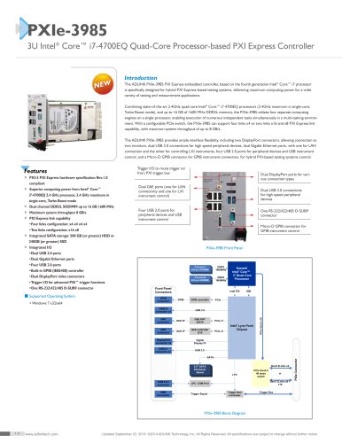
General-Purpose Timer/Counter
■t Number of channels: 1
■t Resolution: 16 Bit
■t Compatibility: 5 V/TTL
■t Base clock available: 2 MHz, external clock to 2 MHz
General Specifications
■t I/O connector
tt · 37-pin D-sub female
tt · 20-pin ribbon male x 2
t ■t Operating temperature: 0˚C to 55˚C (32˚F to 131˚F)
t ■t Storage temperature: -20˚C to 80˚C (-4˚F to 176˚F)
t ■t Relative humidity: 5% to 95%, non-condensing
t ■t Power requirements
t
+5 V
600 mA typical
+12 V
100 mA typical
t ■t Dimensions (not including connectors)
tt 175 mm x 107 mm (6.82” x 4.17”)
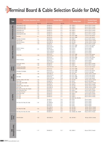
Terminal Boards & Cables
■tDIN-37D-01*
t Terminal Board with One 37-pin D-sub tt
t Connector and DIN-Rail Mounting
■tDIN-20P-01*
t Terminal Board with One 20-pin Ribbon tt
t Connector and DIN-Rail Mounting
■tACLD-9137-01
t General-Purpose Terminal Board with One 37-pin
t D-sub Male Connector
* Cables are not included. For information on mating cables,
refer to P3-48/49.
Ordering Information
■tPCI-9114DG
t 32-CH 16-Bit 100 kS/s Normal-Gain Multi-Function DAQ Card
■tPCI-9114A-DG
t 32-CH 16-Bit 250 kS/s Normal-Gain Multi-Function DAQ Card
■tPCI-9114A-HG
t 32-CH 16-Bit 250 kS/s High-Gain Multi-Function DAQ Card
Isolated Digital Output
t ■t Number of channels: 16
t ■t Output type: open emitter Darlington transistors
t ■t Sink current
tt · 350 mA for one channel @ 100% duty
tt · 260 mA for all channels @ 10% duty
t ■t Power dissipation: Max. 1.47 W per chip (8 DO channels)
t ■t Supply voltage: 5-35 V
t ■t Isolation voltage: 2500 VRMS
t ■t Data transfers: programmed I/O
t
t
Power Output
■t Output voltage: +12 V and -12 V
■t Resettable fuse protection: 500 mA
Updated September 23, 2014. ©2014 ADLINK Technology, Inc. All Rights Reserved. All specifications are subject to change without further notice.
www.adlinktech.com 3-26
"