عضویت
عضویت  ورود اعضا
 راهنمای خرید


StratoSPHERE Plasma System0 pages
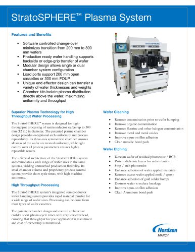
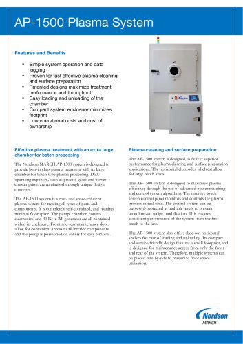
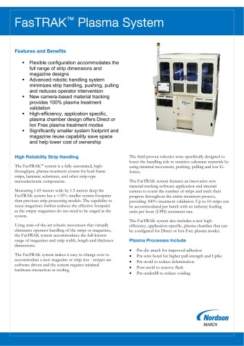
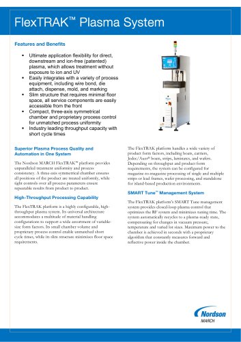
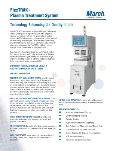
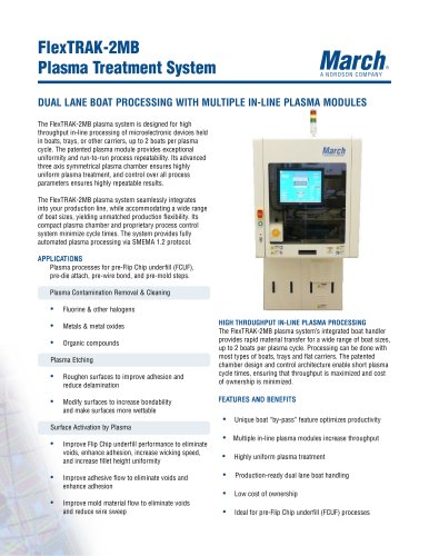
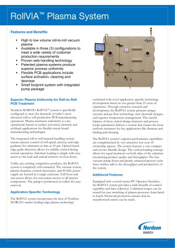
StratoSPHERE™ Plasma System
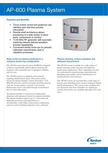
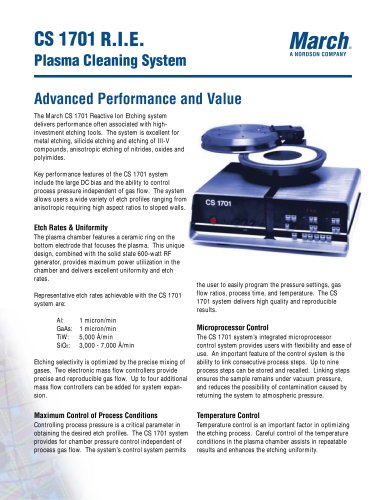
Features and Benefits
Software controlled change-over
minimizes transition from 200 mm to 300
mm wafers
Production ready wafer handling supports
backside or edge-grip transfer of wafer
Modular design allows single or dual
chamber system configuration
Load ports support 200 mm open
cassettes or 300 mm FOUP
Unique end effector design can transfer a
variety of wafer thicknesses and weights
Chamber kits isolate plasma distribution
directly above the wafer, maximizing
uniformity and throughput
Superior Plasma Technology for High
Throughput Wafer Processing
The StratoSPHERE™ system is designed for highthroughput processing of semiconductor wafers up to 300
mm (12 in.) in diameter. The patented plasma chamber
design provides exceptional etch uniformity and process
repeatability. Its three-axis symmetrical chamber ensures
all areas of the wafer are treated uniformly, while tight
control over all process parameters ensures highly
repeatable results.
The universal architecture of the StratoSPHERE system
accommodates a wide range of wafer sizes in the same
systems, yielding unmatched production flexibility. Its
small chamber volume and proprietary process control
system provide short cycle times, with high machine
autonomy.
High Throughput Processing
The StratoSPHERE system’s integrated semiconductor
wafer handling system provides rapid material transfer for
a wide range of wafer sizes. Processing can be done from
most types of wafer cassettes.
The patented chamber design and control architecture
enables short plasma cycle times with very low overhead,
ensuring that throughput for your application is maximized
and cost of ownership is minimized.
Wafer Cleaning
Remove contamination prior to wafer bumping
Remove organic contamination
Remove fluorine and other halogen contamination
Remove metal and metal oxides
Improve spun-on film adhesion
Clean metallic bond pads
Wafer Etching
Descum wafer of residual photoresist / BCB
Pattern dielectric layers for redistribution
Strip / etch photoresist
Enhance adhesion of wafer applied materials
Remove excess wafer applied mold / epoxy
Enhance adhesion of gold solder bumps
Destress wafer to reduce breakage
Improve spun-on film adhesion
Clean Aluminum bond pads