عضویت
عضویت  ورود اعضا
 راهنمای خرید


AltaSight Specifications0 pages

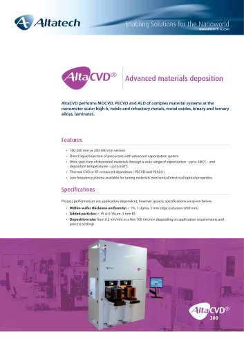
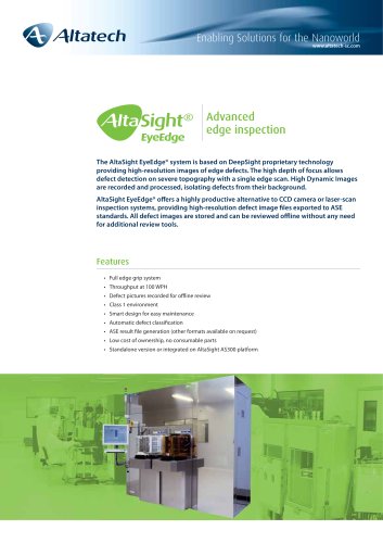
untitled table.main {} tr.row {} td.cell {} div.block {} div.paragraph {} .font0 { font:8.00pt "Lucida Sans Unicode", sans-serif; } .font1 { font:10.00pt "Lucida Sans Unicode", sans-serif; } .font2 { font:12.00pt "Lucida Sans Unicode", sans-serif; } .font3 { font:14.00pt "Lucida Sans Unicode", sans-serif; } .font4 { font:16.00pt "Lucida Sans Unicode", sans-serif; } .font5 { font:24.00pt "Lucida Sans Unicode", sans-serif; } .font6 { font:19.00pt "Palatino Linotype", serif; } ^pAltatech ■ h-speed fer inspection AltaSight® is based on a unique, patented full-field optical technology. This enables a high-efficiency inspection equipment concept at high throughput. AltaSight® SL300 offers technology for whole surface inspection (frontside, backside and edge). From wafer lapping to final inspection or incoming quality check, this unique technology combination grants you a wide point of view on your wafer or process. itures 300 mm, full wafer coverage Օ Throughput at 100 WPH Topographical sensitivity in nanometer range Օ Class 1 measurement chamber Smart design for easy maintenance Օ Defect map correlation between wafer frontside and backside ASE and KLARF output support Օ Defect picture recording for offline review Low cost of ownership i *
"