
 عضویت
عضویت  ورود اعضا
 راهنمای خرید


LOADING

the SD-2 : Silicon to Glass Bonding Wafers Brochure0 pages
نسخه متنی
"
"
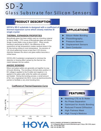
| SD-2 Glass Substrate for Silicon Sensors | |||||||||||||||||||||||||||||||||||||||||
| PRODUCT DESCRIPTION | |||||||||||||||||||||||||||||||||||||||||
| HOYA's SD-2 substrate is designed with a coefficient of thermal expansion curve which closely matches Si single crystal. THERMAL EXPANSION PROPERTIES Borosilicate glass has been widely used as a bonding material to Silicon Wafer. CTE curves of Borosilicate glass and Silicon Single Crystal Wafer cross at about 240LC. When anodic bonding is performed at 400LC, the difference of the expansions at high temperature creates residual stress ill the Si chip during cooling to room temperature. As precision of LSI circuit patterning moves to less than 0.25 microns, distortion between the silicon and glass wafers becomes a critical issue. | |||||||||||||||||||||||||||||||||||||||||
| APPLICATIONS | |||||||||||||||||||||||||||||||||||||||||
| ► Silicon Wafer Bonding ► Photolithography ► Pressure Sensors ► Displacement Sensors ► Semi Conductor | |||||||||||||||||||||||||||||||||||||||||
| HOYA's SD-2 substrate is engineered to minimize the distortion or bowing effect caused by the thermal mismatch between the two wafers. ANODIC BONDING Silicon and glass wafers are generally put together by way of Anodic Bonding. This bonding is formed when positive (+) DC voltage is applied to the Si wafer and negative (-) is applied to the glass wafer while the wafers are pressed and heated. During the bonding process, a small amount of Na+ ions, engineered into SD-2, move as electroconductive carriers to facilitate a very short bonding time. | |||||||||||||||||||||||||||||||||||||||||
| Coefficient of Thermal Expansion Curve | |||||||||||||||||||||||||||||||||||||||||
| 45 r | |||||||||||||||||||||||||||||||||||||||||
| FEATURES | |||||||||||||||||||||||||||||||||||||||||
| 40 | |||||||||||||||||||||||||||||||||||||||||
| ► Matching CTE to Si Wafer ► No Phase Separation ► Optimized for Anodic Bonding ► Reduced Fresnel Diffraction ► High Flatness Mask ► High Young's Modulus | |||||||||||||||||||||||||||||||||||||||||
| 2" o X LU I- | |||||||||||||||||||||||||||||||||||||||||
| 35 | |||||||||||||||||||||||||||||||||||||||||
| 30 | |||||||||||||||||||||||||||||||||||||||||
| 0 | 100 | 200 | 300 T (LC) | 400 | 500 | 600 | |||||||||||||||||||||||||||||||||||
| -HOYA | |||||||||||||||||||||||||||||||||||||||||
| HOYA CANDEO OPTRONICS CORPORATION 2-1-2,Nagaoka,Mizuho-machi,Nishitama-gun,Tokyo,190-1232,Japan TEL +81-42-568-7830 FAX +81-42-568-7791 | |||||||||||||||||||||||||||||||||||||||||


