عضویت
عضویت  ورود اعضا
 راهنمای خرید


ASIC0 pages

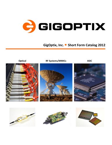
GigOptix is now offering ASIC Solutions
ASIC Families
Configurable Configurable
Structured ASIC (SA)/Platform ASIC features include:
Configurable
Memory Blocks
I/Os
Complete Design Services
● RAM & RAMBIST Generation
● PLL Specification
● Test Bench Generation
● JTAG & Boundary Scan Insertion
● Floorplanning
● Simulation
● Pre‐validated mixed‐signal PHYs and PLLs
● Up to 500 signal I/O’s configurable in metal
● Fully configurable logic & memory structures
● XPath conversion to Standard Cell
● Available for 0.35u, 0.25u, 0.18u & 0.13u designs
Ideal for:
● Risk mitigation with complex mixed‐signal IP’s, such as USB & PCI Express
● Rapid implementation & fabrication of complex designs
Platform/Structured ASIC
● Low NRE and low to mid‐volume designs
● Cost reduction of expensive FPGAs
Hybrid ASIC (HA) features include:
Memory Blocks
Standard Cell Logic
Configurable
● Standard Cell performance with structured ASICs benefits
Logic Cells
● Broad portfolio of Digital, Analog, and Mixed‐Signal IP
● Available for 0.13μ and 65nm processes
Ideal for:
● Cost‐sensitive, high‐performance designs that require certain
functions to be modifiable for derivative products
● Fast prototypes and low NRE of derivative products
● Applications with encryption, video compression, pre‐standard
implementations, data acquisition protocols, & more
Standard Cell Logic
Hybrid ASIC
Memory Blocks
Standard Cell (SC)/ SoC features include:
Memory
Blocks
● Broad portfolio of Digital, Analog, & Mixed‐Signal IP
● Available for 0.25μ, 0.18μ, 0.13μ and 65nm for digital and mixed signal designs
● Available for 0.8μ, 0.6μ, 0.35μ and 0.18μ for high‐voltage (HV) analog designs
Analog Block
Ideal for:
Logic Cells
Mixed‐Signal Design Flow
●
●
●
●
●
Complete Database
Ready (RTL, Constraints,
Pinout, Test Vectors)
IP Portfolio Summary
● Cost‐sensitive, high‐performance, low power & analog turnkey designs
Standard Cell/SoC
XPath Proven Conversion from Structured ASIC to Standard Cell
Seamless Structured ASIC to Standard Cell conversion. Migrate to Standard Cell for economic optimization and
continuity in production.
Meets
Timing?
Functions Test
ATPG/BIST Test
Vector Simulations Vector Simulations
GigOptix
Synthesis
Customer
Joint
SCAN/JTAG/BIST
Insertion
High‐Speed
Interfaces
I/O & Interfaces
USB 2.0 OTG PHY
USB 2.0 controller
PCI Express 1.1 PHY
PCI Express controller
2.5Gb/s SerDes
MIL‐STD‐1553 controller
CAN controller
Design Signoff by
Customer & Tapeout
Converters
Power & Analog
10‐bit Pipeline ADCs up to 160Msps
12‐bit Pipeline ADCs up to 100 Msps
10‐bit Current Steering DACs
up to 210 Msps
12‐bit Current Steering DAVs
up to 210 Msps
14‐bit SAR ADCs
12‐bit Delta Sigma DACs
Video AFE
LVCMOS
HSTL
SSTL 1.5V, 1.8V, 2.5V, 3.3V
SSTL for DDR & DDRII
LVDS up to 1Gbps
LVPECL
DDR PHY up to 500 Mb/s
DDRII PHY up to 800 Mb/s
MDDR PHY up to 500 Mb/s
Low noise amplifiers
Comparators
Op‐Amps
Analog Switches
Analog Multiplexers
Self‐Calibrated &
On‐Die Termination
PLLs/DLLs
Regulators
Band Gap Reference
Charge Pumps
Power on Reset
Vol. 2, 2010
No
Yes
8‐bit 8051
32‐bit BA12 & BA22
32‐bit ARM7/9
DDR & DDRII controllers
SDRAM controller
Flash/SRAM controller
OTP memory
PCI/PCIX I/O & controllers
10/100/1000 Ethernet MAC
16550 UART, timer, GPIO
3DES/AES encryption
Place & Route
Design Review w/
Linting Rpt. Constraints
Review Design Intention
Back Annotation
Static Timing Analysis
Fabrication
Test
Assembly & Packaging
CPU & Subsystems
Floorplanning Review
with Customer
Analysis
Report/
Feedback
RTL Analysis &
Linting
Netlist Approval
by Customer
RLT Modifications
by Customer
RTL
Handoff