عضویت
عضویت  ورود اعضا
 راهنمای خرید


NIKON L200 AND L300 FOR WAFER APPLICATIONS0 pages

In partnership with:
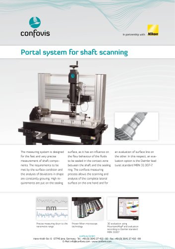
Wafer Microscope NIKON L200/L300
3D measurement system for the surface inspection of wafers
The confovis system NIKON L200
or L300 is particularly suitable
for the detailed measurement
of wafers in the semiconductor
industry. The wafer microscope
systems supply razor-sharp
details and precise measurements
down to the nanometre range.
For professional handling and
Measurements down into
Nanometer Range
perfect positioning, wafer disks
are used in combination with
micro-positioning stages. In this
way, precious data regarding the
surface details of wafers can be
determined in the development,
in testing or directly in the production. The measuring system
solves classical measuring tasks
Fast 3D Analysis
such as roughness, topology or
microgeometry measurements
down to depth resolution in the
nanometre range. With a measuring and working range of 200 or
300 mm, the confovis measuring
system has been designed for
typical wafer sizes.
Precise Micro Positioning
Reliable NIKON components
confovis GmbH
Hans-Knöll-Str. 6 · 07745 Jena, Germany · Tel.: +49 (0) 3641 27 410 -00 · Fax: +49 (0) 3641 27 410 -99
E-Mail: info@confovis.com · www.confovis.com