عضویت
عضویت  ورود اعضا
 راهنمای خرید


UV Light0 pages
OPTICS
Engineer’s know-how
UV Light
DEMANDS ON OPTICAL SYSTEMS
Ultraviolet light is being used more and more in many high-tech applications such as semiconductor processing. Optical components and systems designed specifically for the UV are
essential in order to use its significant potential benefits. Optical engineers must therefore
have design knowledge appropriate to the UV and also be proficient in the technologies used
to manufacture and test UV optics.
THOMAS THOENISS
STEFAN MEWES
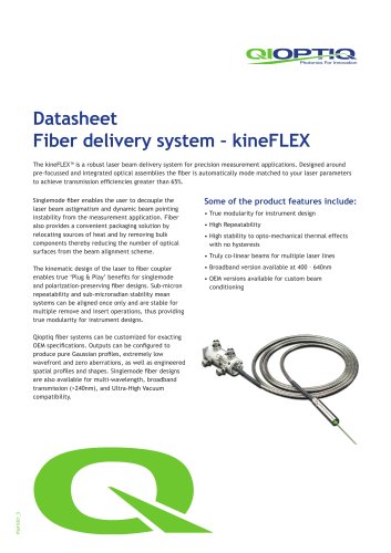
ptical systems working with ultraviolet (UV) light below approximately
400 nm have typically been used for
the optical detection of electric discharge
(solar-blind method), criminalistics (crime
scene inspection) or spectroscopic analytics. Over the past few years, however, UV
light has also taken over other classic optical system applications, for example, industrial inspection or laser material processing.
Another high-tech field, microchip processing, could not be imagined without UV
light. The search for larger storage capacities using smaller semiconductor structures
is intimately linked with the use of light of
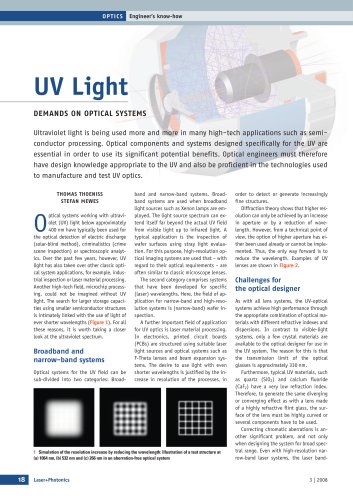
ever shorter wavelengths (Figure 1). For all
these reasons, it is worth taking a closer
look at the ultraviolet spectrum.
O
Broadband and
narrow-band systems
Optical systems for the UV field can be
sub-divided into two categories: Broada
b
band and narrow-band systems. Broadband systems are used when broadband
light sources such as Xenon lamps are employed. The light source spectrum can extend itself far beyond the actual UV field
from visible light up to infrared light. A
typical application is the inspection of
wafer surfaces using stray light evaluation. For this purpose, high-resolution optical imaging systems are used that – with
regard to their optical requirements – are
often similar to classic microscope lenses.
The second category comprises systems
that have been developed for specific
(laser) wavelengths. Here, the field of application for narrow-band and high-resolution systems is (narrow-band) wafer inspection.
A further important field of application
for UV optics is laser material processing.
In electronics, printed circuit boards
(PCBs) are structured using suitable laser
light sources and optical systems such as
F-Theta lenses and beam expansion systems. The desire to use light with even
shorter wavelengths is justified by the increase in resolution of the processes, in
c
1 Simulation of the resolution increase by reducing the wavelength: Illustration of a test structure at
(a) 1064 nm, (b) 532 nm and (c) 266 nm in an aberration-free optical system
18
Laser+Photonics
order to detect or generate increasingly
fine structures.
Diffraction theory shows that higher resolution can only be achieved by an increase
in aperture or by a reduction of wavelength. However, from a technical point of
view, the option of higher aperture has either been used already or cannot be implemented. Thus, the only way forward is to
reduce the wavelength. Examples of UV
lenses are shown in Figure 2.
Challenges for
the optical designer
As with all lens systems, the UV-optical
systems achieve high performance through
the appropriate combination of optical materials with different refractive indexes and
dispersions. In contrast to visible-light
systems, only a few crystal materials are
available to the optical designer for use in
the UV system. The reason for this is that
the transmission limit of the optical
glasses is approximately 330 nm.
Furthermore, typical UV materials, such
as quartz (SiO2) and calcium fluoride
(CaF2) have a very low refraction index.
Therefore, to generate the same diverging
or converging effect as with a lens made
of a highly refractive flint glass, the surface of the lens must be highly curved or
several components have to be used.
Correcting chromatic aberrations is another significant problem, and not only
when designing the system for broad spectral range. Even with high-resolution narrow-band laser systems, the laser band-
3 | 2008