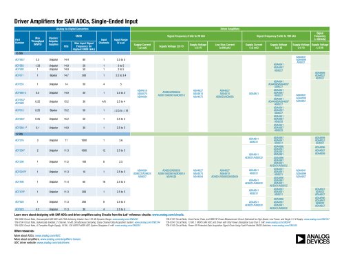
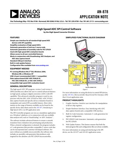
عضویت
عضویت  ورود اعضا
 راهنمای خرید


ADA4177-2: OVP and EMI Protected, Precision, Low Noise and Bias Current Op Amp Data Sheet0 pages
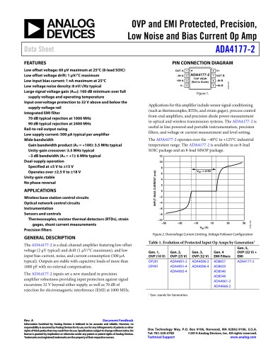
OVP and EMI Protected, Precision,
Low Noise and Bias Current Op Amp
ADA4177-2
Data Sheet
PIN CONNECTION DIAGRAM
OUT A 1
TOP VIEW
(Not to Scale)
V+
7
ADA4177-2
+IN A 3
OUT B
6
–IN B
5
V– 4
+IN B
Figure 1.
Applications for this amplifier include sensor signal conditioning
(such as thermocouples, RTDs, and strain gages), process control
front-end amplifiers, and precision diode power measurement
in optical and wireless transmission systems. The ADA4177-2 is
useful in line powered and portable instrumentation, precision
filters, and voltage or current measurement and level setting.
The ADA4177-2 operates over the −40°C to +125°C industrial
temperature range. The ADA4177-2 is available in an 8-lead
SOIC package and an 8-lead MSOP package.
12
10
8
APPLICATIONS
Wireless base station control circuits
Optical network control circuits
Instrumentation
Sensors and controls
Thermocouples, resistor thermal detectors (RTDs), strain
gages, shunt current measurements
Precision filters
VSY = ±15V
6
4
2
0
–2
–4
–6
–30
–10
10
30
VIN (V)
50
12282-446
–8
–10
–50
Figure 2. Overvoltage Current Limiting, Voltage Follower Configuration
GENERAL DESCRIPTION
The ADA4177-2 is a dual-channel amplifier featuring low offset
voltage (2 µV typical) and drift (1 µV/°C maximum), and low
input bias current, noise, and current consumption (500 µA
typical). Outputs are stable with capacitive loads of more than
1000 pF with no external compensation.
Table 1. Evolution of Protected Input Op Amps by Generation 1
Gen. 1,
OVP (10 V)
OP291
OP491
The ADA4177-2 inputs set a new standard in precision
amplifier robustness providing input protection against signal
excursions 32 V beyond either supply, as well as 70 dB of
rejection for electromagnetic interference (EMI) at 1000 MHz.
1
Rev. A
8
–IN A 2
INPUT BIAS CURRENT (mA)
Low offset voltage: 60 µV maximum at 25°C (8-lead SOIC)
Low offset voltage drift: 1 µV/°C maximum
Low input bias current: 1 nA maximum at 25°C
Low voltage noise density: 8 nV/√Hz typical
Large signal voltage gain (AVO): 100 dB minimum over full
supply voltage and operating temperature
Input overvoltage protection to 32 V above and below the
supply voltage rail
Integrated EMI filter
70 dB typical rejection at 1000 MHz
90 dB typical rejection at 2400 MHz
Rail-to-rail output swing
Low supply current: 500 µA typical per amplifier
Wide bandwidth
Gain bandwidth product (AV = +100): 3.5 MHz typical
Unity-gain crossover: 3.5 MHz typical
−3 dB bandwidth (AV = +1): 6 MHz typical
Dual-supply operation
Specified at ±5 V to ±15 V
Operates over ±2.5 V to ±18 V
Unity-gain stable
No phase reversal
12282-001
FEATURES
Gen. 2,
OVP (25 V)
ADA4091-2
ADA4091-4
ADA4092-4
Gen. 3,
OVP (32 V)
ADA4096-2
ADA4096-4
Gen. 4
EMI Filters
AD8657
AD8659
AD8546
AD8548
ADA4661-2
ADA4666-2
Gen. 5,
OVP (32 V) +
EMI
ADA4177-2
Gen. stands for Generation.
Document Feedback
Information furnished by Analog Devices is believed to be accurate and reliable. However, no
responsibility is assumed by Analog Devices for its use, nor for any infringements of patents or other
rights of third parties that may result from its use. Specifications subject to change without notice. No
license is granted by implication or otherwise under any patent or patent rights of Analog Devices.
Trademarks and registered trademarks are the property of their respective owners.
One Technology Way, P.O. Box 9106, Norwood, MA 02062-9106, U.S.A.
Tel: 781.329.4700
©2014 Analog Devices, Inc. All rights reserved.
Technical Support
www.analog.com