عضویت
عضویت  ورود اعضا
 راهنمای خرید


MICROSCOPY HYPERSPECTRAL IMAGER IMA0 pages
5795 DE GASPE AVENUE, #222
MONTREAL, QUEBEC, H2S 2X3
CANADA
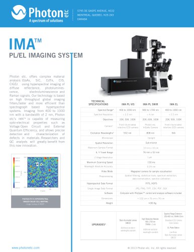
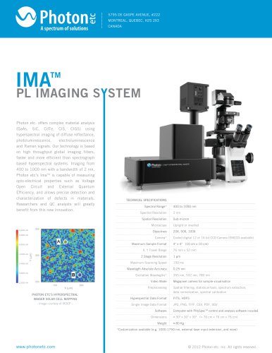
IMA
TM
PL IMAGING SYSTEM
Photon etc. offers complex material analysis
(GaAs, SiC, CdTe, CIS, CIGS) using
hyperspectral imaging of diffuse reflectance,
photoluminescence,
electroluminescence
and Raman signals. Our technology is based
on high throughput global imaging filters,
faster and more efficient than spectrograph
based hyperspectral systems. Imaging from
400 to 1000 nm with a bandwidth of 2 nm,
Photon etc’s ImaTM is capable of measuring
opto-electrical properties such as Voltage
Open Circuit and External Quantum
Efficiency, and allows precise detection and
characterization of defects in materials.
Researchers and QC analysts will greatly
benefit from this new innovation.
TECHNICAL SPECIFICATIONS
Spectral Range*
Spectral Resolution
Spatial Resolution
Microscope
350
5,500E+04
Objectives
5,200E+04
Camera*
Maximum Sample Format
4,600E+04
4,000E+04
Y (μm)
X, Y Travel Range
300
Z Stage Resolution
Maximum Scanning Speed
3,400E+04
Wavelegth Absolute Accuracy
2,800E+04
2,200E+04
Excitation Wavelegths*
250
Video Mode
150
X (μm)
PHOTON ETC’S HYPERSPECTRAL
IMAGER SOLAR CELL MAPPING
- image courtesy of IRDEP -
200
Preprocessing
Hyperspectral Data Format
Single Image Data Format
Software
Dimensions
Weight
400 to 1000 nm
2 nm
Sub-micron
Upright or inverted
20X, 50X, 100X
Cooled digital 12 or 16 bit CCD Camera (EMCCD available)
4" x 4" (10 cm x 10 cm)
76 mm x 52 mm
1 μm
150 ms
0.25 nm
355 nm, 532 nm, 780 nm
Megapixel camera for sample vizualisation
Spatial filtering, statistical tools, spectrum extraction,
data normalization, spectral calibration
FITS, HDF5
JPG, PNG, TIFF, CSV, PDF, SGV
Computer with PHySpecTM control and analysis software incuded
≈ 30" x 30" x 30" (≈ 76 cm x 76 cm x 76 cm)
≈ 80 Kg
*Customization available (e.g. 1000-1750 nm, external laser input extension, and more)
www.photonetc.com
© 2012 Photon etc. Inc. All rights reserved.
"